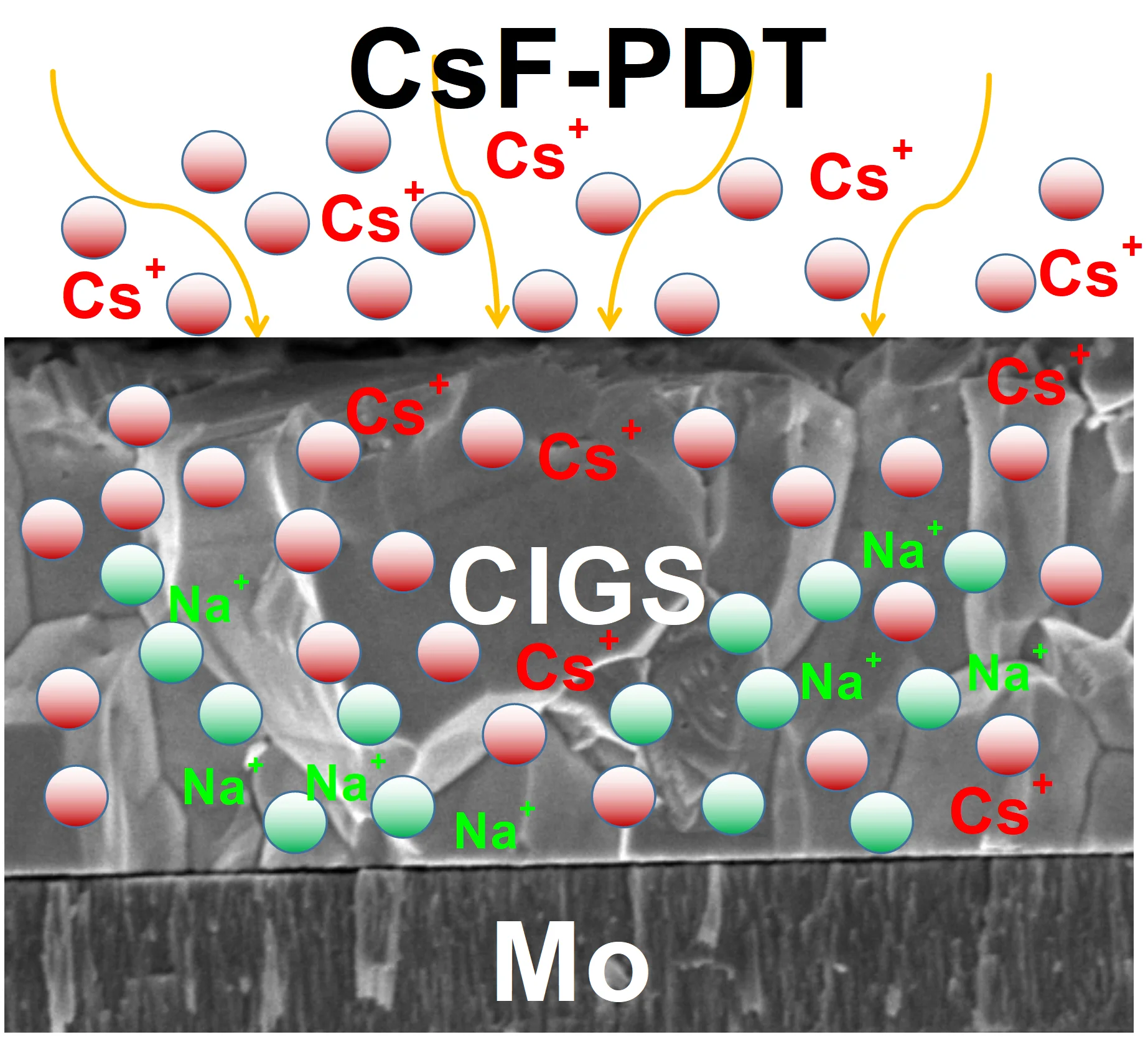
Abstract
In recent years, the device performance of Cu(In,Ga)Se2 (CIGS) solar cells has been improved by heavy alkali element post-deposition treatment (Alkali-PDT). Therefore, it is of great significance to study the mechanism of enhancing CIGS device performance through Alkali-PDT. One aspect to be studied is the distribution of heavy alkali elements in the absorber. In this work, the distribution of the heavy alkali element Cs in the absorber after post deposition treatment of CsF (CsF-PDT) and its effect on the device performance are investigated. The experimental results indicate that Cs can enter both the grain interior (GI) and grain boundaries (GB) via the Cu vacancy (VCu). By comparing the distribution of Na and Cs in the film, it can be noticed that Na is mainly distributed at the GB, while Cs is not differently distributed between the GB and GI. This is mainly due to the fact that the presence of Na at GB inhibits the accumulation of Cs there. The distribution of Cs is beneficial in improving the device’s performance by passivating defects, such as InCu.
Highlights
- Cs mainly diffuses into CIGS films via copper vacancy (VCu) after CsF-PDT.
- Cs can be distributed in grains (GI) and grain boundary (GB) of the films after CsF-PDT.
- The presence of Na at the GB of the film will affect the distribution of Cs at GB.
1. Introduction
In recent years, the efficiency of CIGS solar cells has been greatly improved through post-deposition treatment of heavy alkali elements (Alkali-PDT). For example, the world record efficiency of CIGS solar cells has been raised to 20.4 % [1], 20.8 % [2], and 21.7 % [3] by using post-deposition treatment of KF (KF-PDT). The post-deposition treatment of RbF (RbF-PDT) has further increased the world record efficiency of CIGS solar cells to 22.6 % [4]. The higher world record efficiency of 23.35 % of CIGS solar cells has been achieved by exploiting post-deposition treatment of CsF (CsF-PDT) [5]. There are numerous investigations into the mechanism of improving CIGS device performance through KF/RbF-PDT. One aspect that enhances device performance is the fact K and Rb (similar to Na) distribute at the grain boundary (GB) and grain interior (GI) of absorbers after KF-PDT and RbF-PDT. This is beneficial for passivating the defects at GB and GI, thereby improving device performance [1, 6-9]. Although CsF-PDT can also aid in improving device performance, its mechanism has been less studied. Cs is an alkali atom with a larger atomic radius compared to Na, K, and Rb. Thus, whether the distribution of Cs and its effect on the device performance after CsF-PDT is similar to that of K and Rb after KF/RbF-PDT merits further investigation. Regarding the distribution of Cs, Lin et al. believe that Cs is distributed at the grain boundary (GB) after CsF-PDT, which can help reduce the recombination of minority carriers at GB, thereby improving device efficiency [10]. However, Khatri et al. suggest that the distribution of Cs in the absorber is related to VCu vacancies, di-vacancies (VCu-VSe), and vacancy clusters, and thus it should not be limited to GB [11]. Meanwhile, Lee et al. believe that Cs can be distributed at both GB and GI, but with a greater concentration at GB [12]. The main reason for the improvement of device performance in the above Cs distribution is that Cs can help reduce the number of deep donor-like defects (such as VSe and InCu) and deep-level acceptor-like defects (such as VIn or CuIn), which is conducive to improving the p-type characteristics of CIGS film as well as the VOC of the devices. Since the distribution of Cs is controversial, this work focuses on the distribution of Cs in the absorber after CsF-PDT and its effect on device performance. Due to the existence of Na, which may influence the distribution of Cs in the film, the Na distribution is also investigated. Based on measurements of Cs distribution within the absorber after CsF-PDT, it is evident that Cs can penetrate both the GI and GB of the film via the VCu. However, the existence of Na can hinder Cs distribution in GB and GI, leading to similar Cs distribution in GB and GI. Meanwhile, Cs that enters the film may serve to passivate defects in both GI and GB, for instance, by consuming InCu compensating donors to form CsCu neutral defects, thereby enhancing device performance.
2. Material and methods
The CIGS thin films were prepared on Mo-covered soda-lime glass substrates by a three-step co-evaporation process, involving the co-evaporation of In, Ga, Cu, and Se [1-2]. The substrate temperature in the first step was 350 ℃, and in the second and third steps was 560℃. In the first step, the (In, Ga)2Se3 layer with a thickness of 1µm was deposited. In the second step, Cu(In, Ga)Se2 and a small amount of Cu2-XSe were formed by co-evaporation of Cu and Se on the surface of the (In, Ga)2Se3 layer. In the third step, In, Ga, and Se were co-evaporated to the surface of Cu(In, Ga)Se2 layers with Cu-rich properties, to transform it into a Cu-poor layer. The thickness of the finished Cu(In, Ga)Se2 (CIGS) films was about 2 μm. Based on the above method, we prepared a set of CIGS films, which contained three samples. We selected one sample without CsF-PDT (No-PDT) and the other two samples with CsF-PDT. In the process of CsF-PDT, the CsF was evaporated under the Se atmosphere for 5 min with a substrate temperature of 450 ℃. The doping amount of CsF was controlled by adjusting the evaporation source temperature (360 °C and 420 °C). After the completion of CsF-PDT, the samples were cleaned in ammonia water with a concentration of 0.5 M for 5 minutes to remove the CsF remaining on the surface of the absorber. Then the absorbers were covered with 50 nm CdS by chemical bath deposition. Finally, the solar cells were finished by depositing an rf-sputtered i-ZnO/ZnO: Al bi-layer front contact with a thickness of 90 nm and 430 nm respectively. The composition of the CIGS film and the related device characteristics are shown in Table 1.
In order to obtain the compositional depth profile of the film, secondary ion mass spectroscopy using SIMS (Cameca, Ims7f) was conducted. The sputtering primary beam was O2+ with an impact energy of 10 keV and the beam current of 100 nA. The scanning area was 250×250 µm2, and the analysis area was a circular area with a diameter of 63 µm. Besides, the structure and cross-section of the CIGS layers were characterized in a Hitachi S-4800 SEM using in-lens detectors with 5 keV acceleration voltage. High-angle annular dark field (HAADF) and element-mapping images were acquired with FEI Talos F200S transmission electron microscope (TEM) at 200 kV. Micro-probe energy dispersive X-ray analysis (EDX) was performed in the scanning mode. The TEM specimens were made using a focused ion beam (FIB) with a micro-sampling system (FEI Dual-Beam Helios 450S) and the thickness of the TEM lamella is around 100 nm. Current density-voltage(J-V) characteristics of the solar cells were obtained under simulated standard test condition (25 ℃, 1000W/m2, AM 1.5G illumination).
3. Results and discussion
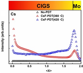
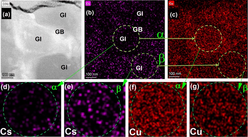
In order to investigate the distribution of Cs in the CIGS film after CsF-PDT, we conduct SIMS measurement and the results are shown in Fig. 1. As can be seen from Fig. 1(a), Cs gradually diffuses from the surface of the absorber to its interior in a gradient form with the increase of CsF deposition. Finally, when CsF evaporation is sufficient (CsF-PDT (420 ℃)), Cs will be evenly distributed within the film. This indicates that the distribution of Cs in the film is related to its doping amount, and Cs can enter the GI and GB of the film. Besides, according to Malitckaya’s first-principles calculation, Cs should diffuse into the film through a copper vacancy (VCu) [13]. Therefore, its distribution should be related to the amount of VCu. To verify the relationship between VCu and distribution of Cs by experiment, we prepare CIGS films (CGI (Cu/(In+Ga))≈0.5) containing a large amount of VCu. Then, the CsF-PDT and TEM tests are performed. TEM-EDX measurements show that Cs is distributed in GI and GB. When Cu content in GI and GB is less, Cs content is more (Fig. 2(b-g)). The experiment results above are consistent with Malitckaya's calculation [11].
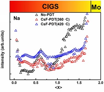
Fig. 1SIMS depth profile of CIGS thin film a) sample Cs, b) sample Na
a)
b)
Fig. 2a) TEM image of the CIGS film and b)-c) TEM-EDX maps of Cs and Cu obtained from the CIGS film. The α and β circles represent enlarged maps of the distribution of d)-e) Cs and f)-g) Cu within the GI
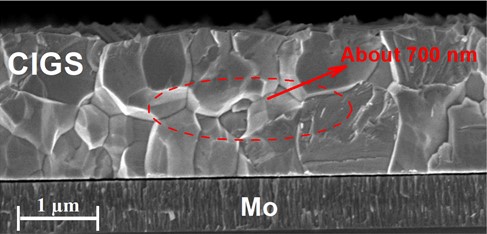
Since CIGS thin films are deposited on the substrate of Mo-coated soda lime glass, a large amount of Na will diffuse from the substrate into it. Therefore, in order to study the distribution of Cs in more detail, we compare it with that of Na. As can be seen from Fig. 1(b), Na can enter the GI and GB of the film and it is more located at about 700 nm near the surface of the absorber before and after CsF-PDT. The further SEM measurement displays that there is a large amount of GB near 700 nm on the surface of the film (Fig. 3). Therefore, we conclude that Na can enter the GB and GI of the film, but it mainly distributes in GB. This is consistent with the result of many researches [14-16]. For instance, F. Couzinie-Devy [15], O. Cojocaru-Miredin[14], and Anke et al. [16]. suggest that Na segregates at GB and GI.
Based on the measurement results above, it can be found that the distribution of Cs is different from that of Na. Na and Cs can both distribute GI and GB. However, Na is mainly distributed in the GB of the film, while Cs is not significant different in the GI and GB (Fig. 1(a)).
Fig. 3Cross-sectional scanning electron microscopy photographs of CIGS film
Cs and Na are both alkali elements, but their distribution in the film is quite different. To clarify this question, we will study the distribution of Na and Cs from two aspects: the way they diffusing into the film and the relationship between them and the defects. It is known that a large number of defects (such as VSe, VCu, InCu, (CuIn+InCu) and (2VCu+InCu)) are formed during the growth of CIGS films. They are distributed in GI and GB, but mainly at GB [17]. Na diffuses from the sodium-lime glass substrate into the film and reacts with these defects during the film growth. Thus, Na is largely distributed at GB [15, 16]. On the contrary, Cs is doped after the CIGS film prepared [18]. According to the measurements above, Cs diffuses into the film through VCu. Therefore, its distribution should be related to the amount of VCu. Since both Na and Cs can occupy VCu and the formation enthalpy of CsCu is higher than that of NaCu[12], the presence of NaCu will hinder the formation of CsCu. By this way, the existence of Na at GI and GB can affect the distribution of Cs [19]. Therefore, GB has more VCu, but Cs can only take up a part of it. This may be the reason why there is no significant difference in Cs distribution between GI and GB after CsF-PDT. According to the analysis above, it can be inferred that Cs can enter into the CIGS film through the VCu vacancy and distribute at GI and GB. However, as a large number of VCu at GB is occupied by Na, the accumulation of Cs at GB decreases.
Table 1Composition of CIGS thin film and photovoltaic parameters of Solar cells with different CsF-PDT in this work
Sample (CIGS) | Thickness (µm) | CGI (±0.05) | GGI (±0.02) | VOC (mV) | JSC (mA) | FF (%) | η (%) |
No-PDT#1 | 2 µm | 0.91 | 0.38 | 622±8 | 33±0.2 | 66.2±0.8 | 13.6±0.3 |
CsF-PDT(360℃)#2 | 2 µm | 0.91 | 0.38 | 694±6 | 33.1±0.2 | 73.4±0.4 | 16.9±0.2 |
CsF-PDT(420℃)#3 | 2 µm | 0.91 | 0.38 | 603±9 | 29.7±0.4 | 62.3±0.6 | 11.2±0.3 |
Cs can enter the film after CsF-PDT, thus it will affect the performance of CIGS devices. As can be seen from Table 1, when the temperature of the CsF source is 360 ℃, the open voltage open-circuit Voltage (VOC), fill Factor (FF), and efficiency () of the device are significantly improved. However, in the case of the CsF source temperature of 420 ℃, the VOC, short-circuit current density (), FF, and of the devices all decrease. The influence of Cs doping on the device performance above may be related to the amount of Cs entering the film and the role it plays. Firstly, Cs entered into the film mainly via VCu, thus in addition to occupying the VCu, they may also consume InCu compensating donors to produce CsCu neutral defects. This is beneficial for improving the hole carrier concentration, thereby enhancing the device’s performance [12]. Secondly, a large number of Cs entering GI may lead to lattice distortion of the film (CsF-PDT(420℃)), which in turn deteriorates the device performance. Therefore, to balance the beneficial and harmful effects of Cs doping, it is necessary to control the doping amount of Cs reasonably.
4. Conclusions
In this paper, the distribution of the heavy alkaline element Cs in the absorber after CsF-PDT and its influence on device performance have been studied. According to the measurement results, it can be found that Cs can enter the grain interiors (GI) and grain boundaries (GB) of the film via vacancies (VCu) after CsF-PDT. By comparing the Na and Cs distributions after CsF-PDT, it can be noticed that Na can distribute at GBs and GIs, but it mainly distributes at GB. It is distributed there by reacting with defects (such as InCu,VCu) at GBs during the growth of the film. Since Cs is doped after the film finished and the formation enthalpy of CsCu is higher than that of NaCu, the presence of Na will hinder the Cs accumulation. This results in a smaller difference in the distribution of Cs at GBs and GIs in CIGS films. In terms of the effect of Cs doping on device performance, it can be found that Cs can help to passivate defects, such as donor-like InCu defects, thereby improving device performance. However, if a large number of Cs enter the GI, it may cause lattice distortion, which is harmful to device performance. Therefore, it is necessary to reasonably control the doping amount of Cs in the film.
References
-
A. Chirilă et al., “Potassium-induced surface modification of Cu(In,Ga)Se2 thin films for high-efficiency solar cells,” Nature Materials, Vol. 12, No. 12, pp. 1107–1111, Nov. 2013, https://doi.org/10.1038/nmat3789
-
P. Jackson, D. Hariskos, R. Wuerz, W. Wischmann, and M. Powalla, “Compositional investigation of potassium doped Cu(In,Ga)Se2 solar cells with efficiencies up to 20.8%,” physica status solidi (RRL) – Rapid Research Letters, Vol. 8, No. 3, pp. 219–222, Feb. 2014, https://doi.org/10.1002/pssr.201409040
-
P. Jackson et al., “Properties of Cu(In,Ga)Se2 solar cells with new record efficiencies up to 21.7%,” physica status solidi (RRL) – Rapid Research Letters, Vol. 9, No. 1, pp. 28–31, Dec. 2014, https://doi.org/10.1002/pssr.201409520
-
P. Jackson, R. Wuerz, D. Hariskos, E. Lotter, W. Witte, and M. Powalla, “Effects of heavy alkali elements in Cu(In,Ga)Se2 solar cells with efficiencies up to 22.6%,” physica status solidi (RRL) – Rapid Research Letters, Vol. 10, No. 8, pp. 583–586, Jul. 2016, https://doi.org/10.1002/pssr.201600199
-
M. Nakamura, K. Yamaguchi, Y. Kimoto, Y. Yasaki, T. Kato, and H. Sugimoto, “Cd-free Cu(In,Ga)(Se,S)2 thin-film solar cell with record efficiency of 23.35%,” IEEE Journal of Photovoltaics, Vol. 9, No. 6, pp. 1863–1867, Nov. 2019, https://doi.org/10.1109/jphotov.2019.2937218
-
R. Kamada, T. Yagioka, S. Adachi, A. Handa, and H. Sugimoto, “New world record Cu(In, Ga)(Se, S)2 thin film solar cell efficiency beyond 22%,” in Photovoltaic Specialists Conference, pp. 1287–1291, 2016.
-
D. Shin et al., “Effects of the incorporation of alkali elements on Cu(In,Ga)Se2 thin film solar cells,” Solar Energy Materials and Solar Cells, Vol. 157, pp. 695–702, Dec. 2016, https://doi.org/10.1016/j.solmat.2016.07.015
-
S. Ishizuka, N. Taguchi, J. Nishinaga, Y. Kamikawa, S. Tanaka, and H. Shibata, “Group III elemental composition dependence of RbF postdeposition treatment effects on Cu(In,Ga)Se2 thin films and solar cells,” The Journal of Physical Chemistry C, Vol. 122, No. 7, pp. 3809–3817, Feb. 2018, https://doi.org/10.1021/acs.jpcc.8b00079
-
P. Schöppe et al., “Rubidium segregation at random grain boundaries in Cu(In,Ga)Se2 absorbers,” Nano Energy, Vol. 42, pp. 307–313, Dec. 2017, https://doi.org/10.1016/j.nanoen.2017.10.063
-
T.-Y. Lin et al., “Alkali-induced grain boundary reconstruction on Cu(In,Ga)Se2 thin film solar cells using cesium fluoride post deposition treatment,” Nano Energy, Vol. 68, p. 104299, Feb. 2020, https://doi.org/10.1016/j.nanoen.2019.104299
-
I. Khatri and M. Sugiyama, “Effect of combined treatment of cesium fluoride as precursor and post-treatment on Cu(In,Ga)Se2 thin film solar cell,” Applied Physics Letters, Vol. 118, No. 11, p. 113901, Mar. 2021, https://doi.org/10.1063/5.0043464
-
H. Lee et al., “Passivation of deep-level defects by cesium fluoride post-deposition treatment for improved device performance of Cu(In,Ga)Se2 solar cells,” ACS Applied Materials and Interfaces, Vol. 11, No. 39, pp. 35653–35660, Oct. 2019, https://doi.org/10.1021/acsami.9b08316
-
M. Malitckaya, H.-P. Komsa, V. Havu, and M. J. Puska, “Effect of alkali metal atom doping on the CuInSe2-based solar cell absorber,” The Journal of Physical Chemistry C, Vol. 121, No. 29, pp. 15516–15528, Jul. 2017, https://doi.org/10.1021/acs.jpcc.7b03083
-
O. Cojocaru-Mirédin, P. Choi, R. Wuerz, and D. Raabe, “Atomic-scale distribution of impurities in CuInSe2-based thin-film solar cells,” Ultramicroscopy, Vol. 111, No. 6, pp. 552–556, May 2011, https://doi.org/10.1016/j.ultramic.2010.12.034
-
F. Couzinie-Devy, E. Cadel, N. Barreau, L. Arzel, and P. Pareige, “Na distribution in Cu(In,Ga)Se2 thin films: Investigation by atom probe tomography,” Scripta Materialia, Vol. 104, pp. 83–86, Jul. 2015, https://doi.org/10.1016/j.scriptamat.2015.03.028
-
A. Laemmle, R. Wuerz, T. Schwarz, O. Cojocaru-Mirédin, P.-P. Choi, and M. Powalla, “Investigation of the diffusion behavior of sodium in Cu(In,Ga)Se2 layers,” Journal of Applied Physics, Vol. 115, No. 15, pp. 387–222, Apr. 2014, https://doi.org/10.1063/1.4871457
-
C. Persson and A. Zunger, “Anomalous grain boundary physics in PolycrystallineCuInSe2: the existence of a hole barrier,” Physical Review Letters, Vol. 91, No. 26, p. 26640, Dec. 2003, https://doi.org/10.1103/physrevlett.91.266401
-
Y. Sun et al., “Review on alkali element doping in Cu(In,Ga)Se 2 thin films and solar cells,” Engineering, Vol. 3, No. 4, pp. 452–459, Aug. 2017, https://doi.org/10.1016/j.eng.2017.04.020
-
S. Cheng et al., “Effects of different Cs distribution in the film on the performance of CIGS thin film solar cells,” Solar Energy Materials and Solar Cells, Vol. 211, No. 1, pp. 110917, 2021, https://doi.org/10.1016/j.solmat.2020.110917
About this article

The work was supported by the Science and Technology Innovation Project of Higher Education Institutions in Shanxi Province (Grant No. 2022L429), the Key R&D Project of Datong City (Grant No. 2020019), Shanxi Datong University doctoral research funding project (Grant No. 2021-B-04).
The datasets generated during and/or analyzed during the current study are available from the corresponding author on reasonable request.
Conceptualization, Funding Acquisition and Supervision are performed by Shiqing cheng and Yun sun. Data Curation, Formal Analysis and Writing – Original Draft Preparation are conducted by Shiqing cheng. Project Administration are performed by Shiqing cheng, Hongmei Liu.
The authors declare that they have no conflict of interest.
