Abstract
Microstructure modifications on thin photoelectrical properties refers to changes in the microscopic structure of thin films that affect their ability to convert light into electricity. This study investigates the deposition and post-treatment effects in the electric and visual qualities of GZO, IZO, and ZnO thin layers, aiming to enhance their applicability in electronic and optoelectronic devices, according to the X-raydiffraction (XRD) examination. Thin films were deposited on glass substrates using magnetic sparking at thicknesses of 300 nm and 500 nm, followed by treatments like wet aging and annealing at 220 °C. The results showed significant improvements in crystallinity and optical characteristics, with ZnO films exhibiting a preferred (003) orientation. IZO films demonstrated notable mobility at 10.96 cm2/V-sec and resistivity of 2.49×10⁻3 ohm-cm. The novelty of this research is the novel integration of wet aging and low-temperature annealing, that notably improves thin film efficiency while maintaining structural integrity. The findings indicate that post-treatment significantly enhances the properties of these thin films, suggesting their potential for various electronic applications.

Highlights
- This study shows that post-treatment techniques such as wet aging and annealing greatly improve ZnO, IZO, and GZO thin-film optical and electrical characteristics.
- The remarkable mobility and low resistivity of IZO films demonstrated their potential for application in cutting-edge electrical and optoelectronic devices
- The results emphasize how important preferred crystallographic orientations are, especially for ZnO films where the orientation improves photoelectrical performance.
1. Introduction
Thin film technology has contributed significantly to the advancement of modern electronics and optical electronics. Thin films are used to make solar panels, LEDs, and light detectors since their thickness can vary from a few nanometers to many micrometers [1]. The performance and effectiveness of the devices are determined by the thin-film microstructure. Changes in the microstructure greatly influence the photoelectric properties of thin films, which have implications for many applications. Materials are modified internally to improve specific properties, a process known as microstructure modification. Defect density, phase distribution, and grain size can all be affected by processes such as alloying and annealing. Thermal stability, electrical conductivity, and mechanical strength are all improved by optimizing these adjustments. For example, specific materials can improve corrosion resistance, while finer grains can increase hardness. Understanding the relationship between microstructure and performance is important for applications as diverse as electronics and aerospace. Change is necessary for the advancement of natural science and technology [2]. The capacity of thin films to convert light into electrical impulses is known as a photoelectric characteristic. These characteristics – namely, the distribution of grains with other particles, form, size, and arrangement – are intrinsically related to the microstructure of the films [3]. Therefore, it was able to greatly improve thin-film devices' performance by comprehending and modifying their microstructure. It is possible to view the complex interaction between microstructure and photoelectric properties. The efficiency of devices like solar cells can be decreased by defect levels in polycrystalline thin films, especially at the grain boundaries, which can serve as recombination hotspots. Microstructure flaws such as vacancies and interstitials that have the potential to pin charge carriers and immobilize them can potentially degrade the photoelectric properties of the film. It enables the modification of the material's electrical properties to suit certain applications [4].
The ability to produce charge carriers, the absorption of light by thin films, and the use of efficient carriers in optical electronics are the reasons for the photoelectric properties of thin films [5]. In electronics, transistors are made of thin sheets and need capacitors to keep devices clean. Additionally, thin films are used in coatings to increase wear resistance, corrosion prevention, and enhance optical quality. Another important feature of the microstructure that significantly affects the penetration and scattering of light in thin films is the surface area [6]. The absorption properties of solar devices can be enhanced by incorporating nanostructures into the solid surface, improving the optical trapping. Thin materials were widely used in LEDs for uniform illumination. For solar devices to be effective, accurate surface alignment is required [7]. In addition to offering an economical substitute for traditional silicon solar panels in photovoltaics, thin film solar cells also open up the prospect of flexible and lightweight designs. Changes in their microstructure significantly affect the performance of thin-film photovoltaic devices. Grain size, phase composition, and defect density can all be varied to improve charge carrier capacity and light absorption. Applications such as solar cells and sensors can be more efficient if these microstructural characteristics are optimized. Researchers can manipulate the microstructure to create desired electro-optical features. In the final analysis, modifications are crucial for the development of thin-film technologies [8].
To investigate the impact of post-treatment deposition processes of the electric and visual qualities in IZO, GZO and ZnO thin layers. By examining these effects, this research aims to improve the performance of films for electro-optoelectronic applications. The main goal of this study is to increase resistivity, mobility and crystallinity. This study aims to determine ideal film quality conditions through focused treatments, to progress the materials' practical application in a range of technical domains.
2. Key contribution
1) This work shows that post-treatment techniques such as wet aging and annealing greatly improve ZnO, IZO, and GZO thin-film optical and electrical characteristics.
2) The remarkable mobility and low resistivity of IZO films demonstrated their potential for application in cutting-edge electrical and optoelectronic devices, therefore improving overall device efficiency.
3) The results emphasize how important preferred crystallographic orientations are, especially for ZnO films where the orientation improves photoelectrical performance.
The following Sections make up the article: Section 2, Related works; Section 3,Deposition and Post-Treatment; In Section 4 discuss the experimental result; and Finally Section 5, Conclusion.
3. Related works
The lower temperature of solvent thermal processes technique was utilized to create ZnO with QDs of average particle size [9]. After employing the spin coating process to create the ZnO with QD-based solution, thin film annealing took place at a certain C. According to the image luminescence examination, it constituted a higher concentration of vacancies in oxygen in both the as-coated and warmed ZnO films. The switching function and exceptional photovoltaic capabilities of arsenic selenide films constitute the usefulness in phase shift storage and solar energy cells [10]. The LM-SFM technique combined the advantages of both methods of connection among the film width and RI and dielectric coefficient.
The spin-coating was utilized to effectively produce thin films of ZnO loaded with Bi [11]. The SEM, EDS, TEM, SAED methods and photoluminescence tests were used to investigate the impacts of the quantity and photoelectric characteristics of films. It focused on creating the antireflection grating structures that compensate for the transmittance of light loss through the coating of layer. Ultrasonic vibrations were aided by laser illumination [12]. To reduce the optical characteristic condition, enhance the beneficial impact of ultrasonic vibration and enable the coherence of beam-excited SP to possess reflected light.
The study examined the effective synthesis of composite oxide films using the sol-gel technique [13]. The powder diffraction, FE-SEM, and ESCA were the characterization methods used to investigate the composite oxide thin film’s crystallographic phase, surface shape, and chemical makeup. The mixture of a heterojunction is created by coating with narrow band gap Bi trioxide using electromagnetic blasting [14]. The reaction of particles inside the material may be inhibited and the inadequate reception of ZnO in the range of visible light can be efficiently compensated for creating a heterostructure modification. The thickness constitutes on hybrid architecture's morphology and electrical structure.
Tin dopants can provide additional conducting particles to increase the terminal levels of ITO for thin films [15]. ITO films made by magnetic sputter were treated with SCCO2 solvent at varying concentrations of solutions. The ITO microscopic structures were interpreted by the photovoltaic efficiency of ITO films as fluid manipulations.
The non-Gaussian form microscale replies of a viscoelastic metal layer evenly exposed by a laser pulse heat flux were taken by the generalized [16] thermo-viscoelastic theory model with fractional relaxation operators. Using the Laplace transform as a technique, the issue has been analytically resolved in the converted domain. The numerical technique based on Fourier transforms can be employed to obtain the inverse transforms. Strategies for expansion. The relationship between viscoelastic property and fractional relaxation operators on the reactions of the metal film has been spoken about and given visual representations.
The governing equations were described using the photo-thermoelasticity theory based on moisture diffusivity [17], and analytical solutions were obtained by applying Laplace transforms. When the conditions thermal ramp type and non-Gaussian plasma shock were applied to the surface numerically using inverse Laplace transforms, complete solutions were achieved linearly in the time domain. To visually represent the fundamental physical quantities being studied, numerical simulation is utilized.
Based on fractional strain theory, the transient response of a rotating rod with a one-dimensional (1D) micro-nano-structured viscoelastic composition under the effect of a moving heat source has been examined, accounting for microscale memory-dependent effects [18].
By employing a time-fractional derivation of level and the time-fractional integral of level , a computational framework for heat and plasma transfer in a natural semiconductor device was created [19]. For half of the space of viscous thin-wall semiconductors, the model solves two-dimensional issues that were traction-free and exposed to an exponentially fading heat pulse using Laplace and Fourier integral transforms.
To investigate if a mixture of two interacting thermoplastic materials gets impacted by an external magnetic field [20]. The analytical harmonic wave solution was used to demonstrate and solve the basic mathematical equations, providing the answer for the problem’s descriptive functions. The 2-D and 3-D mixture of the two interreacted thermoelastic materials with mutual temperature was found to have clear displacements and stresses. It was examined and talked about. Everywhere, the functions’ found solution was finite.
Propose a fresh extended model of a micropolar theory [21] that integrated the concept of a memory-dependent derivative (MDD) with a Dual-phase lag thermoplastic model (DPL). The Laplace transform method was used to solve the governing equations analytically, removing the time-dependent derivatives. The broad distributions of the various thermophysical fields under consideration were then determined by applying numerical Laplace inversion to obtain the numerical results for the problem’s physical quantities. Ultimately, a comprehensive analysis and graphical display of the numerical outcomes were offered.
4. Deposition and post-treatment of thin films
ZnO, IZO, and GZO thin films with thicknesses of 300 and 500 nm were magnetically spark-deposited into glass substrates. To improve their structural, optical, and electromagnetic qualities, the films were post-treated using annealing and wet aging after deposition. The goals of these procedures were to enhance crystallization and lessen flaws. In the end, careful deposition combined with sophisticated post-treatments produced high-grade thin films appropriate for a range of photoelectric and electrical uses.
4.1. Deposition process
Thin films of ZnO, IZO, and GZO were deposited on substrates of glass by magnetic sparking, with respective thicknesses of 300 nm and 500 nm. The method used targets made of ZnO, IZO, and GZO with a circumference of 5 inches. The operational state was kept at torr during the period of deposition, whereas the base pressure of the container was kept at torr. Combining a turbo pump with an engine that rotates the method used to reach the volume levels. To guarantee uniform film growth, the sparking intensity was adjusted to 160 W through the film installation process.
4.2. Post-treatment procedures
The films were subjected to further treatments after deposition to improve their characteristics and functionality. Wet aging and sterilizing are two processes. To increase the films’ electromagnetic and optical qualities, decrease flaws, and enhance crystallization, annealing usually entails heating films to a particular temperature. Wet aging is a technique that may be used to shape or sanitize the film surfaces by selectively removing portions of the thin films using a solution of chemicals.
The ZnO, IZO, and GZO films that were stored on glass underwent post-treatments to evaluate and enhance the visual, electronic, and structural properties. Sophisticated post-treatments along with regulated deposit conditions were used to create high-quality thin films appropriate for a range of photoelectric and electronic functions.
5. Experimental results
This section describes the experimental setup for producing ZnO, IZO, and GZO films, as well as the evaluation of their structural, optical, and electrical characteristics following different treatments and aging procedures. A thorough discussion of the findings, comprising surface morphology, crystallinity, light absorption, and electrical properties, follows.
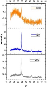
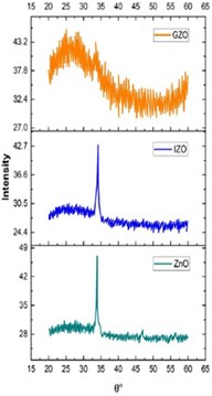
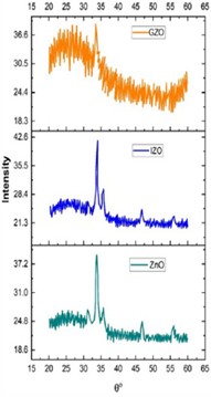
ZnO, IZO, and GZO films (300 nm thick) were post-treated with 45 minutes of normalization at 220 °C and 10 minutes of stripping in sodium hydroxide. All films exhibited smooth, well-crystallized surfaces. The 300 nm GZO film was smooth, whereas the 500 nm GZO film contained void flaws. Despite variations in thickness, the ZnO and IZO films (300 and 500 nm) had continuous surfaces. XRD spectra verified crystallinity in both 300 and 500 nm films, implying a pure ZnO composition. Figs. 1(a, b, c) emphasize the structural features, surface texture, and crystallinity, demonstrating the films' softness and excellence after synthesis.
Fig. 1Films at 300 nm: a) scored, b) normalized and c) untreated
a)
b)
c)
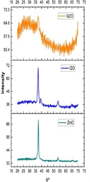
Fig. 2, depicts the properties of 500-nm-thick synthetic IZO sheets. Fig. 2(a), emphasizes surface textures and possible flaws, whereas Fig. 2(b), depicts smooth, continuous surfaces after normalization, proving efficient synthesis. Fig. 2(c), shows untreated films with crystalline structures, which were verified by XRD examination. Despite processing differences, the figures show that the IZO films are effective at synthesis and have structural integrity.
Fig. 2Films at 500 nm: a) engraved, b) normalized and c) untreated
a)
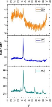
b)
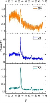
c)
Peak intensity is affected by the aging procedure, with dry aging resulting in characteristic ZnO peaks showing pristine crystalline structure. Wet aging raised peak power, indicating higher crystallinity or morphological variations. ZnO films had a (003) favored orientation, whereas GZO films had decreased crystallinity. Arsenic in IZO films caused higher interruption than aluminum. Film thickness and processing techniques influenced the crystallographic characteristics of ZnO, IZO, and GZO films.
During wet aging, IZO films showed strong (003) and (102) peaks, but GZO films did not. The hydroxide surroundings impacted the orientation of the IZO film. Radiofrequency magnetron sputtering produced pure ZnO films with a variety of orientations. Wet aging improved the crystal orientation of IZO films (003) while weakening the (102) peak. This shows the impact of aging on IZO film crystallinity, which is important for applications. The random atomic arrangement of the glass substrate impacted the crystal growth orientation in ZnO, IZO, and GZO films.
The (003) peak intensity indicates a preferred crystallographic orientation, which varied with aging procedures. Aging aligned initially random grains, raising peak intensity along the (003) axis, showing better structural alignment. These results emphasize the significance of aging conditions in enhancing crystal arrangements in ZnO, IZO, and GZO thin films for transistors and optical systems.
5.1. 300 nm films of ZnO, IZO, and GZO's coefficient of light absorption spectrum
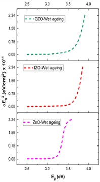
Fig. 3, shows the photonic band gap spectra of untreated 300 nm ZnO, IZO, and GZO films. First, each material’s band gap was determined. During dry aging, ZnO’s band gap reduced slightly, IZO's raised and GZO's stayed constant. Wet aging increased the band gap for IZO, held constant for ZnO, and remained constant for GZO. These findings demonstrate how aging impacts the visual characteristics of these films, which influences their application in electronics.
The first band gaps of ZnO, IZO, and GZO were determined on 500 nm films. The band gap of ZnO broadened after dry aging, while that of IZO and GZO raised. Wet aging resulted in wider band gaps. These results show how aging and doping fluctuations impact the band gap activity of ZnO, IZO, and GZO films, as illustrated in Fig. 3.
Fig. 3Films at 300 nm: a) no aging, b) dry aging, and c) wet aging
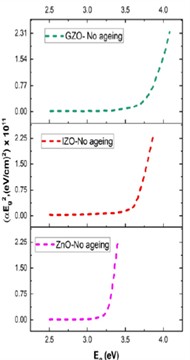
a)
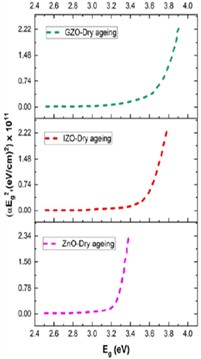
b)
c)
Heavily doped n-type transistors increase electrical concentration, moving the Fermi level into the conduction band and widening the band gap. As a result, light penetrates deeper and shorter-wavelength photons are more efficiently absorbed. GZO films had a wider band gap than ZnO and IZO, increasing luminescence penetration. Figs. 3-4 show the optical characteristics of films treated with potassium chloride and atmospheric circumstances, with a film penetration rate reduced by 6 %. Transmission () is affected by attenuation coefficient () and thickness (), which affects film absorption.
Film thickness and absorbance have a negative correlation. Light is attenuated mainly through reflection and diffusion, with an important absorbance at 490 nm. Beyond 500 nm, the films enable substantial energy transfer in the visual spectrum, but they primarily absorb near 490 nm, near to the UV range. Impurity density, flaws, interface smoothness, and grain borders all have an impact on light diffusion, with contaminants and grain boundaries contributing significantly to decreased penetration.
Air annealing enhanced the crystal structure by raising light transfer at shorter wavelengths and visual light emission. Annealing also increased carrier density, which lowered the absorption threshold to shorter wavelengths. Alkaline solution treatments changed the film’s band gaps, impacting efficiency. Post-treatment improved the films’ optical characteristics, increasing light transmission, lowering diffusion losses, and increasing their effectiveness for electronic uses.
5.2. 500 nm films of ZnO, IZO, and GZO’s coefficient of light absorption spectrum
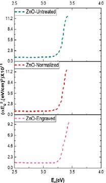
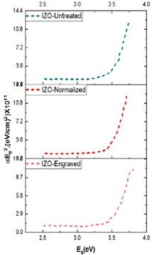
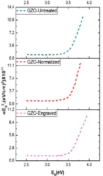
This study examines the 500 nm thick ZnO, IZO, and GZO films under different aging processes, as shown in Fig. 4, The electromagnetic transfer in IZO and GZO films is mainly caused by oxygen vacancies and transitional atoms. ZnO films with non-stoichiometric compositions exhibit higher electrical conductivity at vacant particle positions. IZO films surpass others in electromagnetic effectiveness, with the smallest resistance and maximum transport density. Raised annealing temperature substantially increases ZnO film resistivity because of oxygen molecules on the surface impeding electron mobility. When oxygen is absorbed, the resulting shortage decreases flaw and electron density, which increases electrical resistance.
The anti-aging features of IZO and GZO films outperform those of ZnO due to doping agents that improve stability and effectiveness. Fig. 4, depicts the features of ZnO, IZO, and GZO films under untreated, normalized, and etched circumstances. Normalized ZnO films are smoother Fig. 4(a), whereas untreated films have unique surface characteristics. Fig. 4(b), depicts distinct textures in etched and normalized IZO films, while Fig. 4(c), shows similar features in GZO films under all circumstances. In summary, the results show that the various treatments have an important impact on the surface morphology and performance of these thin films.
Fig. 4500 nm films of untreated, normalized and engraved: a) ZnO, b) IZO and c) GZO
a)
b)
c)
Following treatment, ZnO films exhibited raised resistance because of oxygen molecule adsorption, which decreased electrical permeability and formed obstacles to electron mobility. The absorbed oxygen acts as a receptor, increasing the film’s permeability while reducing the density of transport agents. In contrast, IZO and GZO films have anti-aging characteristics, rendering them better suited for uses that require long-term durability. Their high conductivity and resistance to ecological deterioration render them suitable for utilization in a variety of electrical and optical devices. The substantial impacts of aging and doping on the morphological and electrical characteristics of ZnO-based films emphasize the significance of carefully choosing dopants and improving post-deposition treatments. This tailoring increases the film's durability and effectiveness. The experimental findings highlight the fundamental procedures that influence film behavior, assisting in the creation of new materials. Tables 1-3, outline the electrical characteristics of IZO, GZO, and ZnO films.
Table 1ZnO electrical characteristics
Properties | ZnO | ||
Wet Ageing test | Untreated | Dry Ageing test | |
Mobility (cm2 / V-sec) | 17.95 | 17.90 | 4.40 |
Resistivity×10-3 (ohm-cm) | 23.07 | 24.63 | 243.90 |
Sheet R (ohms per square) | 769.0 | 958.5 | 8130.0 |
Carrier concentration×1019 (cm-3) | 1.51 | 1.42 | 0.58 |
Table 2IZO electrical characteristics
Properties | IZO | ||
Wet Ageing test | Untreated | Dry Ageing test | |
Mobility (cm2 / V-sec) | 10.96 | 11.03 | 21.72 |
Resistivity×10-3 (ohm-cm) | 2.49 | 2.25 | 0.66 |
Sheet R (ohms per square) | 83.1 | 85.8 | 22.1 |
Carrier concentration×1019 (cm-3) | 22.84 | 25.19 | 43.34 |
Table 3GZO electrical characteristics
Properties | GZO | ||
Wet Ageing test | Untreated | Dry Ageing test | |
Mobility (cm2 / V-sec) | 4.53 | 5.71 | 6.55 |
Resistivity×10-3 (ohm-cm) | 12.24 | 11.13 | 12.24 |
Sheet R (ohms per square) | 408.0 | 803.3 | 135.0 |
Carrier concentration×1019 (cm-3) | 11.25 | 9.81 | 23.53 |
5.3. Discussion
The study examines the effect of deposition and post-treatment techniques on the electrical and optical characteristics of GZO, IZO, and ZnO thin films, with an emphasis on their applicability for electronic and optoelectronic uses. Magnetic sparking was used to form thin films on glass substrates with thicknesses of 300 nm and 500 nm, which were then treated with wet aging and annealing at 220 °C. The results show that variations in the microstructure of these thin films have a direct impact on their capacity to transform light into electricity, as verified by X-ray diffraction (XRD) examination. ZnO films had a preferred (003) orientation, suggesting increased crystallinity, that is important for enhancing efficiency. Table 1 demonstrates a substantial decrease in mobility for ZnO films during dry aging, with values dropping to 4.40 cm2/V-sec compared to 17.95 cm2/V-sec in the wet aging test, with a dramatic increase in resistivity from 23.07×10⁻³ ohm-cm in wet aging to 243.90×10⁻³ ohm-cm in dry aging. In contrast, IZO films showed an optimal mobility of 10.96 cm2/V-sec and resistivity of 2.49×10⁻³ ohm-cm in the wet aging test (Table 2). This indicates their better electrical efficiency and possibility for practical uses. GZO films have comparable electrical properties to IZO films, with a mobility of 4.53 cm2/V-sec and consistent resistivity values (Table 3). However, they are less strong. Overall, the research highlights the importance of improving deposition and post-treatment procedures in order to customize the characteristics of these thin films to particular functionalities, highlighting the possibility of ZnO, IZO, and GZO in improving electronic devices.
6. Conclusions
Films of ZnO, IZO, and GZO were created by RF magnetron blasting. The following findings are supported by analytical outcomes. The IZO film showed that angular particles were more crystalline. The GZO film's consistency was inadequate due to its gaps. All the films display the (002) favored position, according to the analysis of XRD. Purified and crystalline ZnO substance like crystal structure was detected on dry aging spectra. Wet aging led to a notable rise in the spectrum’s spikes’ lower levels of intensity. Where 500-900 nm wavelengths, the coatings constitute a coefficient of penetration at 91 %. The optical spectrum band gaps of ZnO, IZO and GZO thin films were obtained with alkaline conditions. The median score rate of penetration were decreased at 6 % as a result of higher contaminants in both wet and dry aging solutions. The electrical characteristics of IZO and GZO films were superior to ZnO film demonstrated. With regard of piece obstructions, transport concentration and resistance, IZO film demonstrated the greatest results. With more intense air annealing, ZnO film impedance increased dramatically. The anti-wrinkle properties of GZO and IZO films were superior to the environment.
The various photoelectric properties that thin films exhibit under various operating conditions may have an impact on their practical value. Integrating thin films into complex devices or systems may provide technical challenges, such as compatibility issues with other materials or interfaces. Future studies should focus on creating thinner-film materials that are more dependable and have longer lifespans by strengthening their stability and resistance to environmental stresses.
References
-
S.-H. Hu, Y.-S. Lin, S.-H. Su, H. Dai, and J.-S. He, “Optimizing the microstructures of inclined deposition to improve the photoelectric properties of ZnO thin films,” Journal of Electronic Materials, Vol. 53, No. 8, pp. 4869–4879, Jun. 2024, https://doi.org/10.1007/s11664-024-11220-8
-
Z. Huang et al., “Effect of oxide layer state on the photoelectric properties of thermally sensitized PbS thin films,” Optical Materials, Vol. 150, p. 115289, Apr. 2024, https://doi.org/10.1016/j.optmat.2024.115289
-
Y. Niu, L. Duan, X. Zhao, C. Han, J. Guo, and W. Geng, “Effect of Sb doping on structural and photoelectric properties of SnO2 thin films,” Journal of Materials Science: Materials in Electronics, Vol. 31, No. 4, pp. 3289–3302, Jan. 2020, https://doi.org/10.1007/s10854-020-02877-y
-
M. Sampath, T. Logu, P. Mathan Kumar, K. Asokan, and K. Sethuraman, “Enhancement of photoelectric properties of Cu2ZnSnS4 thin films by electronic excitations induced by swift heavy ions,” Materials Science and Engineering: B, Vol. 280, p. 115683, Jun. 2022, https://doi.org/10.1016/j.mseb.2022.115683
-
F. Mei, J. Huang, T. Yuan, and R. Li, “Effect of cerium doping on the microstructure and photoelectric properties of Ce-doped ITO films,” Applied Surface Science, Vol. 509, p. 144810, Apr. 2020, https://doi.org/10.1016/j.apsusc.2019.144810
-
P. Lv et al., “The influence of scattering layer thin film on photoelectric properties of Bi2S3/CdS/TiO2 electrode,” Vacuum, Vol. 161, pp. 21–28, Mar. 2019, https://doi.org/10.1016/j.vacuum.2018.12.018
-
Z. Li et al., “Preparation and photoelectric properties of silver Nanowire/ZnO thin film ultraviolet detector,” Electronic Materials Letters, Vol. 19, No. 5, pp. 415–423, Mar. 2023, https://doi.org/10.1007/s13391-023-00421-8
-
E. Acosta, “Properties and applications,” in Thin Films, IntechOpen, 2021, https://doi.org/10.5772/intechopen.95527
-
A. T. Nomaan, A. A. Ahmed, N. M. Ahmed, M. I. Idris, M. R. Hashim, and M. Rashid, “ZnO quantum dot based thin films as promising electron transport layer: influence of surface-to-volume ratio on the photoelectric properties,” Ceramics International, Vol. 47, No. 9, pp. 12397–12409, May 2021, https://doi.org/10.1016/j.ceramint.2021.01.094
-
X.-L. Liu et al., “Effect of thickness of antimony selenide film on its photoelectric properties and microstructure,” Chinese Physics B, Vol. 32, No. 2, p. 027802, Feb. 2023, https://doi.org/10.1088/1674-1056/ac8724
-
B. Hou et al., “Influence of Bi3+ doping on microstructure and photoelectric properties of ZnO thin film,” Chemical Physics Letters, Vol. 763, p. 138174, Jan. 2021, https://doi.org/10.1016/j.cplett.2020.138174
-
Y.-Y. Wang, B.-J. Li, L.-J. Huang, H.-D. Cao, and N.-F. Ren, “Photoelectric property enhancement of Ag/FTO thin films by fabricating antireflection grating structures using ultrasonic-vibration-assisted laser irradiation,” Applied Surface Science, Vol. 541, p. 148449, Mar. 2021, https://doi.org/10.1016/j.apsusc.2020.148449
-
J. Li, X.-G. Tang, Q.-X. Liu, Y.-P. Jiang, and W.-H. Li, “Enhancement of the photoelectric properties of composite oxide TiO2-SrTiO3 thin films,” Advanced Composites and Hybrid Materials, Vol. 5, No. 2, pp. 1557–1565, Apr. 2021, https://doi.org/10.1007/s42114-021-00237-w
-
Y. Nie et al., “Preparation of ZnO/Bi2O3 composites as heterogeneous thin film materials with high photoelectric performance on FTO base,” Coatings, Vol. 11, No. 9, p. 1140, Sep. 2021, https://doi.org/10.3390/coatings11091140
-
Z. Liu et al., “Enhancement in photoelectric properties of ITO films by regulating defects and dopants with supercritical fluid treatment,” Applied Surface Science, Vol. 565, p. 150551, Nov. 2021, https://doi.org/10.1016/j.apsusc.2021.150551
-
M. H. Hendy, M. A. Ezzat, and M. M. Amin, “Wave propagation due to laser irradiation in viscoelastic thin metal film with fractional relaxation operator,” Materials Physics and Mechanics, Vol. 48, No. 1, Jan. 2022, https://doi.org/10.18149/mpm.4812022_4
-
M. A. Ezzat, “Hyperbolic thermal-plasma wave propagation in semiconductor of organic material,” Waves in Random and Complex Media, Vol. 32, No. 1, pp. 334–358, Jan. 2022, https://doi.org/10.1080/17455030.2020.1772524
-
M. H. Hendy, M. M. Amin, and M. A. Ezzat, “Memory-dependent derivative theory of ultrafast laser-induced behavior in magneto-thermo-viscoelastic metal films,” Indian Journal of Physics, Vol. 95, No. 6, pp. 1121–1130, Jun. 2020, https://doi.org/10.1007/s12648-020-01783-7
-
M. A. Ezzat, “A novel model of fractional thermal and plasma transfer within a non-metallic plate,” Smart Structures and Systems, Vol. 27, No. 1, pp. 73–87, Jan. 2021, https://doi.org/10.12989/sss.2021.27.1.073
-
M. A. Ezzat, A. S. El-Karamany, A. A. El-Bary, and M. A. Fayik, “Fractional ultrafast laser-induced magneto-thermoelastic behavior in perfect conducting metal films,” Journal of Electromagnetic Waves and Applications, Vol. 28, No. 1, pp. 64–82, Jan. 2014, https://doi.org/10.1080/09205071.2013.855616
-
M. A. Ezzat, A. S. El-Karamany, and M. A. Fayik, “Fractional ultrafast laser-induced thermo-elastic behavior in metal films,” Journal of Thermal Stresses, Vol. 35, No. 7, pp. 637–651, Jul. 2012, https://doi.org/10.1080/01495739.2012.688662
About this article
The authors have not disclosed any funding.
The datasets generated during and/or analyzed during the current study are available from the corresponding author on reasonable request.
The authors declare that they have no conflict of interest.
