Abstract
Present work deals with the numerical investigation of a cantilever beam having I cross section made up of piezoelectric material for its actuation capability. The beam is modeled under the assumption of Euler’s Bernoulli equation. Eight cases are considered for different electrode locations. The beam was subjected to voltage loads at different locations. It was noticed that tip deflection increases with increasing applied voltage across the electrodes. Maximum tip deflection was achieved with the increase in voltage with particular electrode arrangement. In this report we have also demonstrated that for downward tip deflection, there are two values of thickness ratio of flange and web for a given tip deflection at a given applied voltage.
1. Introduction
In the last few years, a number of actuators has been developed for various applications [1-6], which are usually driven by the electrostatic, thermal, piezoelectric and electromagnetic methods. There have been many research papers on the subject of piezoelectric sensors and actuators [7-9]. Some of the work focused on the accuracy and efficiency of the numerical procedures used for the modeling. In case of actuation, the electrical variables are exchanged into mechanical variables. In many applications, the actuators are highly desired to provide large displacements of several tens of micrometers with a small voltage below 10 V. Xindong et al. [10] presented a novel actuator which is driven by Lorentz force provided 55 μm displacement with the diving current of 8 mA. Most piezoelectric actuator use unimorph structures which have been realized in cantilevers, bridges or membranes [11] to generate large deflections. L. Q. Yao et al. [12] provide the static behaviors of piezoelectric cantilever actuator under large electric field. It shows that as the magnitude of the electric field increases, the tip deflection increases. PengGao et al. [13] designed a micro- actuator which is capable of providing in-plane flexibility and out of plane stiffness. Piezoelectric actuation has become widespread in micromanipulation systems where high positioning accuracy is needed [14]. Beyond their properties in the sense of micromechatronic design, an advantage of using piezoelectric material is its reversible electromechanical effect. This explains its high potential use in the microrobotic field as actuators and sensors [15, 16]. Atul and Vinayak [17] reported the numerical investigation of a cantilever having an array of PZT with silicon proof mass. The performance of output voltage with respect to thickness, length and width of PZT pattern was analyzed. The modeling of piezoelectric cantilever beam with 31 effects was also investigated and reported by Vinayak and Atul [18]. The performance of output voltage was examined with different proof mass as well as without proof mass. The effect of different lengths of cantilever beam upon tip deflection was also investigated. Vinayak and Satya [19] reported the numerical investigations of a cantilever having T cross section made of piezoelectric material for its actuation capabilities. They have also demonstrated that for downward deflection, there are two values of thickness ratio of flange and web for a given tip deflection at a given applied voltage. Actuators deploying piezoelectric thin films are very attractive source because of its potential to offer higher output force at lower voltage as compared to other actuators [11, 20-22].
The focus of present work is to investigate the effect of electrode locations on the actuation capability of I cross section piezoelectric cantilever beam. The effect of flange and web thickness on tip deflection is also investigated.
2. Methodology
2.1. Generalized Hamilton’s principle for a piezoelectric beam
According to Hamilton’s principle [23]:
where, T is total kinetic energy; U– total potential energy; We – electrical energy can be given as:
where, [ξ] is vector of mechanicaldisplacements; [S] is vector of mechanical strain components; [σ] is vector of mechanical stress components; [D] is vector of electrical displacement components; [E] is vector of electrical field components; ρ is mass density; Vp is volume of piezoelectric material and t represents transpose of the matrix.
If a set of discrete mechanical forces [f] is applied at locations (xi, yi) and a set of discrete electric charge output [q] is extracted at locations (xi, yi), then variation of mechanically appliedand electrically extracted work may be written as:
where, nf is number of discrete mechanical forces; φi – scalar electrical potential; nq – number of discrete electrode pairs.
The linear electrostatic constitutive equation for piezoelectric material is given by [24]:
where, [c] is elastic stiffness matrix; [e] is matrix of piezoelectric constants; [ε] is matrix of permittivity components
Superscript E and S denote that the parameters are measured at constant electric field and constant strain respectively. Putting Eq. (6) in Eq. (1), the generalized Hamilton’s principle for piezoelectric cantilever beam can be given as:
+∫Vpδ[E]t[εS][E]dVp+∑nfi=1δ[ξ](xi,yi,t)[f](xi,yi,t)+∑nqj=1δφ(xi,yi,t)q(xi,yi,t)]dt=0.
2.2. Piezoelectric electromechanical model
A four node rectangular element with degree of freedoms per node as u, v, w in x, y and z directions is used to model the I cross section piezoelectric cantilever beam. Based upon Euler- Bernoulli’s beam theory, the displacements field is then given by:
where, the displacement components u, v and w at thickness level z from the reference (neutral) surface are given in terms of the transverse deflection (w) of the reference surface. Hence the rectangular element is having 12 structural degree of freedom. It is assumed that each finite element of piezoelectric layer is completely covered with perfectly conductive electrodes on the top and bottom surface and therefore are electrical degree of freedom (voltage Vp across the electrode) is sufficient for modeling the electrical response of the element taken. Thus, the rectangular element has 13 degree of freedom in total.
The mechanical strain components under the assumption of linear strain displacement can be given by:
The transverse displacement of any node k of the finite elements is assumed to vary in the polynomial form i.e.:
where, [P] is polynomial matrix; {μ} is generalized coordinates.
The bending rotation about x axis can be given as:
The polynomial matrix is given as:
Considering 4 nodes per element and 3 degree of freedom per nodes, one can defines 12×1 vector of nodal displacement as:
This can be expressed as:
where, [A] is 12×12 transformation matrix whose elements are given by [P] and its derivatives through the definitions of wk, and θxk is given in Eq. (10) and Eq. (11).
The transverse deflection as a function of nodal variable then can be given by:
where:
The vector of transverse displacement and cross-section rotation is related to the vectors of nodal variable as:
Similarly, the vector of curvature can be expressed as:
Since piezoelectric material is poled in the thickness direction (z direction), the non- zero electric field component (which is assumed to be uniform in thickness direction) can be expressed as:
where the electric field potential is assumed to varying linearly across the electrodes i.e. the electric fields assumed to be uniform in z direction and hp is piezoelectric material thickness. Then the electrode field vector can be written as:
where:
Based upon Hamilton’s principle given by Eq. (7) the element matrix [m], stiffness matrix [k], electromechanical coupling matrix [θ], capacitance cp and the mechanical forcing vector [f] can be expressed as:
[θ]=∫Vp[Z][Bk]t[e]tdVp,cp=∫Vp[BE]t[εS][BE]dVp,[f]=∫s[N]tfwdS,
where:
As the width and thickness of piezoelectric cantilever is small as compared to length, therefore the stress components σ2 and σ3 may be neglected.
Hence the constitutive equation may be expressed as:
The piezoelectric and dielectric component in Eq. (20) are given in contracted notations (i.e. Voigt’s notation) where 1, 2 and 3 directions are coincident with x, y and z directions.
The global equations of motion are then obtained by assembling the element matrices given by Eq. (19) i.e:
where, [M] is global mass matrix; [K] is global stiffness matrix; [Ʊ] is global electromechanical couplingmatrix; [cp] is diagonal global capacitance matrix; {v} is the global vector of voltage outputs; [Q] is global vector of electric charge outputs; [C] is global damping matrix
3. Validation of results
For validation, published results of R. Ly et al. [26] have been used. R. Ly has used piezoelectric cantilever beam having rectangular cross-section. The beam is subjected to 0.01 N excitation forces at the free end of cantilever. The length of beam considered is 49 mm having thickness 0.6 mm and width 3.8 mm respectively. Figs. 1 to 4 shows the comparison of published results with that of present work by finite element method (FEM). Figs. 1 and 2 shows the harmonic response for the first mode in terms of tip displacement and voltage generated of piezoelectric cantilever beam under excitation force of 0.01 N at tip and coefficient of damping assumed is 0.05. Similarly, Figs. 3 and 4 show the harmonic response for the second mode in terms of tip displacement and voltage generated of piezoelectric cantilever beam. From Figs. 1-4, a good agreement in results has been observed between experiment and present work by using the same methodology as considered for I cross section piezoelectric cantilever beam.
4. Modeling procedure
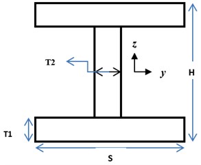
The model cross section of the I cantilever beam is shown in Fig. 5.
The length of beam is 15 mm in all cases. The width of the beam ‘S’ is 5 mm and the height of the beam ‘H’ is 2 mm. The web thickness is ‘T2’ while the flange thickness is ‘T1’ having dimensions 1 mm and 0.5 mm respectively. Piezoelectric material considered is PZT 4. The density of the material taken is 7500 kg/m3. The I cross section beam is cantilevered at one end and is free at the other end. The voltage is applied at different electrode locations at the cross section of the beam as shown in Fig. 6.
Fig. 1Harmonic response in terms of tip displacement (1st mode)
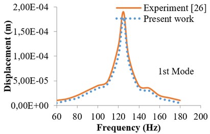
Fig. 2Harmonic response in terms of voltage (1st mode)
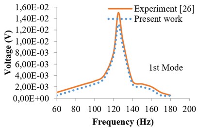
Fig. 3Harmonic response in terms of tip displacement (2nd mode)
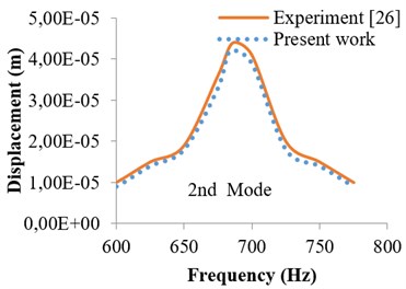
Fig. 4Harmonic response in terms of voltage (2nd mode)
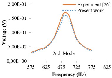
Fig. 5Schematic diagram of I cross section cantilever beam
5. The fem model
For simulation of the piezoelectric phenomenon SOLID5– 3D solid elements are used which has 8-node brick elements. The beam consists of five thousand elements. The electromechanical constitutive equations for linear model behavior are the same as Eq. (6). The matrices of the model containing piezoelectric elements are given by Eqs. (21) and (22). For proper definition of the material, it is necessary to give the piezoelectricity matrix, the electrical permittivity matrix and the anisotropic stiffness matrix. The material properties of materials are given by Table 1.
Fig. 6Different electrode location of I cross section bean. V = Voltage Applied and G = Ground
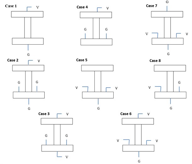
Table 1Materials properties of the piezoelectric cantilever beam
Density | 7500 | kg/m3 |
Stiffness constant | ||
c11 | 13.2×10¹⁰ | N/m2 |
c12 | 7.3×10¹⁰ | N/m2 |
Piezoelectric constant | ||
e31 | –4.1 | C/m2 |
Dielectric constant | ||
ε33 | 804.6 | |
Fig. 7Meshing diagram
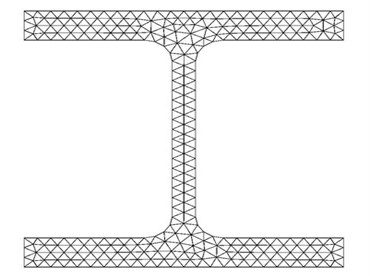
Fig. 8Deformed piezoelectric cantilever beam
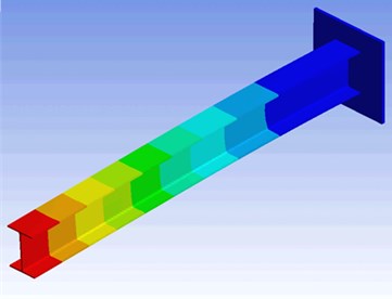
The meshing diagram of I cross-section piezoelectric cantilever beam is shown in Fig. 7. The deformation of I cross-section piezoelectric cantilever beam is shown in Fig. 8. The I cross-section beam in itself is an optimized structure which provides strength over the whole span of beam. Different cases of electrodes locations are taken into consideration. But with a particular arrangement of electrodes at a given applied voltage on I cross-section piezoelectric cantilever beam shows the maximum deflection where energy could be harvested.
6. Numerical results and discussion
The following Table 2 depict the variation of tip deflection of I cross section cantilever for different flange thickness (T1) and web thickness (T2) for different test cases under varying applied voltages as depicted in Fig. 2. {(+) = downward deflection, (-) = upward deflection}.
Table 2Variation of tip deflection keeping cross section area constant and varying applied voltage
CASE – 1 | CASE – 2 | ||||||||||
S. No. | H (mm) | T1 (mm) | T2 (mm) | Voltage (V) | Deflection (+) (mm) | S. No. | H (mm) | T1 (mm) | T2 (mm) | Voltage (V) | Deflection (+) (mm) |
1 | 2 | 0.5 | 1 | 2 | 0.00051 | 1 | 2 | 0.5 | 1 | 2 | 0.00173 |
2 | 2 | 0.5 | 1 | 4 | 0.00103 | 2 | 2 | 0.5 | 1 | 4 | 0.00347 |
3 | 2 | 0.5 | 1 | 6 | 0.00155 | 3 | 2 | 0.5 | 1 | 6 | 0.00521 |
4 | 2 | 0.5 | 1 | 8 | 0.00206 | 4 | 2 | 0.5 | 1 | 8 | 0.00695 |
5 | 2 | 0.5 | 1 | 10 | 0.00258 | 5 | 2 | 0.5 | 1 | 10 | 0.00896 |
CASE – 3 | CASE – 4 | ||||||||||
S. No. | H (mm) | T1 (mm) | T2 (mm) | Voltage (V) | Deflection (+) (mm) | S. No. | H (mm) | T1 (mm) | T2 (mm) | Voltage (V) | Deflection (+) (mm) |
1 | 2 | 0.5 | 1 | 2 | 0.068 | 1 | 2 | 0.5 | 1 | 2 | 0.00207 |
2 | 2 | 0.5 | 1 | 4 | 0.136 | 2 | 2 | 0.5 | 1 | 4 | 0.00415 |
3 | 2 | 0.5 | 1 | 6 | 0.204 | 3 | 2 | 0.5 | 1 | 6 | 0.00623 |
4 | 2 | 0.5 | 1 | 8 | 0.273 | 4 | 2 | 0.5 | 1 | 8 | 0.00896 |
5 | 2 | 0.5 | 1 | 10 | 0.341 | 5 | 2 | 0.5 | 1 | 10 | 0.0103 |
CASE – 5 | CASE – 6 | ||||||||||
S. No. | H (mm) | T1 (mm) | T2 (mm) | Voltage (V) | Deflection (-) (mm) | S. No. | H (mm) | T1 (mm) | T2 (mm) | Voltage (V) | Deflection (-) (mm) |
1 | 2 | 0.5 | 1 | 2 | 0.0678 | 1 | 2 | 0.5 | 1 | 2 | 0.0642 |
2 | 2 | 0.5 | 1 | 4 | 0.135 | 2 | 2 | 0.5 | 1 | 4 | 0.128 |
3 | 2 | 0.5 | 1 | 6 | 0.203 | 3 | 2 | 0.5 | 1 | 6 | 0.192 |
4 | 2 | 0.5 | 1 | 8 | 0.272 | 4 | 2 | 0.5 | 1 | 8 | 0.257 |
5 | 2 | 0.5 | 1 | 10 | 0.340 | 5 | 2 | 0.5 | 1 | 10 | 0.321 |
CASE -7 | CASE -8 | ||||||||||
S. No. | H (mm) | T1 (mm) | T2 (mm) | Voltage (V) | Deflection (-) (mm) | S. No. | H (mm) | T1 (mm) | T2 (mm) | Voltage (V) | Deflection (-) (mm) |
1 | 2 | 0.5 | 1 | 2 | 0.066 | 1 | 2 | 0.5 | 1 | 2 | 0.0339 |
2 | 2 | 0.5 | 1 | 4 | 0.132 | 2 | 2 | 0.5 | 1 | 4 | 0.0678 |
3 | 2 | 0.5 | 1 | 6 | 0.198 | 3 | 2 | 0.5 | 1 | 6 | 0.101 |
4 | 2 | 0.5 | 1 | 8 | 0.264 | 4 | 2 | 0.5 | 1 | 8 | 0.135 |
5 | 2 | 0.5 | 1 | 10 | 0.330 | 5 | 2 | 0.5 | 1 | 10 | 0.169 |
For cases 1, 2, 3 and 4, tip deflections are downward which are assumed as positive and for cases 5, 6, 7 and 8 the tip deflections are upward, which are negative. From the Table 2, it is evident that when voltage applied increases, the tip deflection increases linearly. This is obvious because of the linear nature of equations assumed.
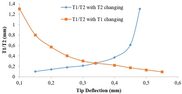
Fig. 9 and 10 have been plotted based on the Table 2 for greater visual clarity. In case 3 and 5, maximum tip deflections have been noted for given applied voltage. The maximum tip deflections have been noted for case 3 (0.341 mm) and case 5 (0.340 mm) for given applied voltage. It is also noteworthy that under applied voltage load of 2 V, the tip deflections for cases 1, 2, and 4 provides minimum deflection. It is further observed from Fig. 10 for a given applied voltage of 2 V, the tip deflection for cases 5, 6 and 7 are approximately same. But with increase in voltage application, tip deflection increases and are maximum for case 3 (downward deflection) and 5 (upward deflection). It indicates that location of electrodes as well as voltage applied play an important role in optimizing the tip deflection of a cantilever. This also suggests that for a given voltage say at 10 V; case 3 and 5 may be a better choice for an actuator. Now case 3 at 10 V has been analyzed for different tip deflections with variation of flange thickness (T1) and web thickness (T2) i.e. (T1/T2) as shown in Fig. 11. It appears from Fig. 11 that at a given applied voltage (say 10 V), a higher tip deflection greater than 0.341 mm is possible with proper T1/T2 value. It is also an important observation from Fig. 11 that for a given tip deflection (say 0.25 mm) at a given applied voltage of 10 V for case 3, we have two values of T1/T2 ratio and therefore two different dimensions of the I cross section piezoelectric cantilever beam are possible.
Fig. 9Variation of tip deflection under applied voltage
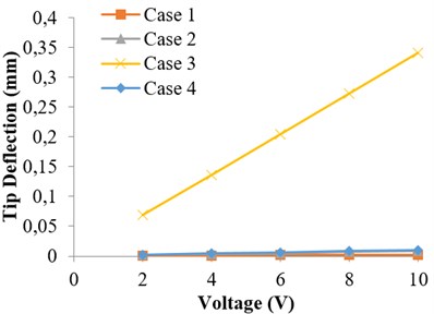
Fig. 10Variation of tip deflection under applied voltage
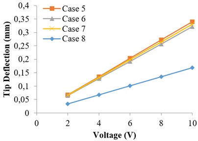
Fig. 11Variation of (T1/T2) ratio on tip deflection
7. Conclusions
Tip deflection increases with increasing applied voltage across the electrode. But higher tip deflection is possible with a particular arrangement of electrodes at a given applied voltage.
For a given downward tip deflection, there are two values of thickness ratio of flange and web at a given applied voltage. The higher tip deflection of 0.47 mm may be obtained with two values of T1/T2 ratio i.e. 0.19 and 1.3 respectively.
References
-
Judy J. W., Muller R. S., Zappe H. Magnetic microactuation of polysilicon flexure structures. Journal of Microelectromechanical Systems, Vol. 4, 1995, p. 162-169.
-
Jeong S. H., Jong S. K., Jan G. K. Structural optimization of a large-displacement electromagnetic Lorentz force microactuator for optical switching applications. Journal of Micromechanics and. Microengineering, Vol. 14, 2004, p. 1585-1596.
-
Grade J. D., Jerman H., Kenny T. W. Design of large deflection electrostatic actuators. Journal of Microelectromechanical Systems, Vol. 8, 2003, p. 2-9.
-
Ko J. S., Lee M. L., Lee D. S., Choi C. A., Kim Y. T. Development and application of laterally driven electromagnetic microactuator. Applied Physics Letters, Vol. 81, 2002, p. 547-549.
-
Qui J., Lang J. H., Slocum A. H., Strümpler R. A high-current electro thermal bi-stable MEMS relay. 16th IEEE International Conference on Micro Electro Mechanical Systems, Kyoto, 2003, p. 64-67.
-
Hwang I. H., Shim Y. S., Lee J. H. Modeling and experimental characterization of the chevron-type bi-stable microactuator. Journal of Micromechanics and Microengineering, Vol. 13, 2003, p. 948-954.
-
Bailey T., Hubbard J. E. Distributed piezoelectric-polymer active vibration control of a cantilever beam. Journal of Guidance, Control and Dynamics, Vol. 8, Issue 5, 1985, p. 605-611.
-
Crawley E. F., de Luis J. Use of piezoelectric actuators as elements of intelligent structures. AIAA Journal, Vol. 10, 1987, p. 1373-1385.
-
Crawley E. F., de Luis J., Hagood N. W., Anderson E. H. Development of piezoelectric technology for application in control of intelligent structures. Proceedings of American Control Conference, 1988, p. 1890-1896.
-
Lv Xingdong, Wei Weiwei, Mao Xu, Chen Yu, Yang Jinling, Yang Fuhua A novel MEMS electromagnetic actuator with large displacement. Sensors and Actuators A: Physical, Vol. 221, 2015, p. 22-28.
-
Maeda R., Tsaur J. J., Lee S. H., Ichiki M. Piezoelectric microactuator devices. Journal of Electroceramics, Vol. 12, 2004, p. 89-100.
-
Yao L. Q., Zhang J. G., Lu L., Lai M. O. Nonlinear static characteristics of piezoelectric bending actuators under strong applied electric field. Sensors and Actuators A, Vol. 115, 2005, p. 168-175.
-
Gao Peng, Yao Kui, Tang Xiaosong, He Xujiang, Shannigrahi Santiranhajn A piezoelectric micro-actuator with a three-dimensional structure and its micro-fabrication. Sensors and Actuators A, Vols. 130-131, 2006, p. 491-496.
-
Breguet J. M., et al. Monolithic piezoceramic flexible structure for micromanipulation. 9th International Precision Engineering Seminar and 4th International Conference on Ultraprecision in Manufacturing Engineering, Braunschweig, Germany, 1997, p. 397-400.
-
Campolo D., Sahai R., Feaing R. S. Development of piezoelectric banding actuators with piezoelectric sensors for micromechanical flapping mechanism. IEEE International Conference on Robotics and Automation, Taipei, Taiwan, 2003, p. 339-46.
-
Branco P. J. C., Dente J. A. On the electromechanics of a piezoelectric transducer using a bimorph cantilever undergoing asymmetric sensing and actuation. Smart Material Structures, Vol. 13, 2004, p. 631-42.
-
Atul, Ranjan Vinayak Design and analysis of piezoelectric cantilever beam with PZT thin films array for vibration energy harvesting. Proceedings of ISSS National Conference on MEMS, Smart Materials, Structures and Systems, Pune, India, 2013.
-
Atul, Ranjan Vinayak, Pandey Ankit L. Finite element modeling of piezoelectric cantilever with 31 effects for sensor application. Sensors and Transducers, Vol. 182, Issue 11, 2014, p. 281-287.
-
Ranjan Vinayak, Chand K. Satya Design and simulation of a piezoelectric T cross section beam as actuator for energy harvesting. Proceedings of International Conference on Smart Materials Structures and Systems, Banglore, India, 2012.
-
Baborowski J. Microfabrication of piezoelectric MEMS. Integrated Ferroelectrics, Vol. 66, 2004, p. 33-51.
-
Lee C., Itoh T., Suga T. Self-excited piezoelectric PZT microcantilevers for dynamic SFM – with inherent sensing and actuating capabilities. Sensors and Actuators A: Physical, Vol. 72, 1999, p. 179-188.
-
Baran U., Brown D., Holmstrom S., Balma D., Davis W. O., Mazzalai A., Muralt P., Urey H. High frequency torsional MEMS scanner for displays. Proceedings of IEEE International Conference Micro Electro Mechanical Systems, Paris, France, 2012, p. 636-639.
-
De Marqui Junior Carlos, Erturk Alper, Inman Daniel J. An electromechanical finite elemnt model for piezoelectric energy harvester plates. Journal of Sound and Vibration, Vol. 327, 2009, p. 9-25.
-
IEEE Group on Sonics and Ultrasonics. The Standards on Piezoelectricity. Institute of Electrical and Electronics Engineer, New York, 1978.
-
Ly R., Rguiti M., D’astorg S., Hajjaji A., Courtois C., Leriche A. Modeling and characterization of piezoelectric cantilever bending sensor for energy harvesting. Sensors and Actuators A: Physical, Vol. 168, 2011, p. 95-100.

