Abstract
The proposed research involves Design and Modeling of Improved Controller (PID), Using DC Source Fed Permanent Magnet Synchronous Motor Drive with Enhanced DC-DC Converter by reducing vibration for Industrial Applications. It consists of a DC-DC converter, voltage-link module, fractional second order system PID controller. In this proposed improved controller, enhanced converter, DC-link switching is achieved by a bridged ripple voltage which results in the improved quality of output power, and it also reduces vibration, and noise in the drive without affecting mechanical properties. Reduction of switches makes the system more cost effective. A simulation of fractional second-order function, Buck-Boost converter is designed, and its concert is analyzed for various functioning factor conditions. The Three-Port Converter and B4-Inverter fed Permanent Magnet Synchronous Motor Drive focused on the industrial applications. An Ampere-hour unit powered converter is used at inductor terminal, which has been realized by minimizing the distortion and decreasing the Ampere-hour unit rating a new topology is proposed. As Comparing with previous system, the proposed system results in the reduced voltage fluctuation at the switches. Hence the proposed system proves power switches are compact, with reduced inrush current and improved output transfer function. Based on this a fulfilling closed loop validation has been performed for both simulation and experimental arrangement.
Highlights
- The tuning process of fractional order PI controller using the SBO algorithm is analyzed.
- To design a fractional order PI controller.
- The larger gain crossover frequency in order to have lower settling time in the closed loop.
- The phase margin should be between 45 degrees and 60 degrees.
- The system possess iso-damping property.
1. Introduction
The intention of the proposed research is to evaluate the performance to test the robustness of the Programmable Integral (PI) system. The different order integrator plus time delay system is taken for the performance analysis from which the system performance can be studied for the effect of the time delay and time constant over the system. Modeling of this system will be useful in order to perform the modeling of the power semiconductor devices for an industrial process using its transfer function. So, the proposed research output for a controller is applied to a low power semiconducting device to get the improved controller output. While coming to power converter, the hostility due to fossil fuel depletion [1] affect outputs. Clean green energy voltage is required. Generally, several single-input/single-output due to complexity their respective cost is high [2-4]. The proposed research focuses on single-input/multi-output (SIMO) converter for increasing efficiency, gain. SIMO proposed in the research is a three-port converter (TPC) which is interfaced with renewable sources, storage elements and loads and simultaneously operates in two stage conversion which efficiency [4-9] is reduced, so the single-stage conversion is implemented. To reduce the power losses further, the TPC architecture is introduced by [10, 11]. The TPC advantage has single-stage conversion connecting any two of the three ports, greater system efficiency and smaller number of components, quick response and included voltage-current management among the ports with a middle power [12-21]. The main objectives of the present research consist in analyzing the controller performance to check the robustness of used PID system. PID loop is applied for a power electronic device with integration of improved converter with less number of power-controlled devices which is regulated with a high quality, in all power flow situations, using various conditions of load for industrial applications. The different order integrator plus time delay system is taken for the performance analysis from which the system performance can be studied for the effect of time delay and time constant over the system. A control system is used in all processes in order to obtain the necessary output by monitoring the system output. A system should possess the following qualities: 1. High accuracy; 2. Sensitive to the input; 3. Bandwidth high and noise free; 4. Transient speed is low with less no. of oscillations; 5. The system remains stable. To get the accurate result, the control system should be closed, and its feedback is compared to that of the open loop system. Since, in a closed loop, the output is sent as a feedback to produce the desired result with high accuracy. Controllers are used for this purpose by tuning the system to produce the desired output from the input as well as to monitor the output. In general, there are three types of controllers: The Proportional controller (P), Integrator controller (I) and Derivative Controller (D) to tune the system output. In the P controller, the output is proportional to the difference between the error and set point signal. It makes the system stable. The P controller suffers from the offset problem and also increases the overshoot of the system. In the integral controller, the output will be the integral value of error with respect to time. This controller has the main advantage of reset back the system to its set point even when the system is disturbed. Hence, it is also called as reset controller. The main disadvantage of the reset controller consists in that it makes the system unstable. The derivative controller cannot be used alone because it produces saturation effects and also amplifies the noise signal produced in the system. Henceforth, the D controller is used as a combination of P, I or both. Tuning of the controller is an important step in designing the system, because it helps the system to reach its desired result. Zeigler and Nichols proposed a design for auto-tuning based on the critical gain and critical frequency of the plant. The problem with this method is that it makes the closed loop system to produce poor robustness. The robustness of the Ziegler’s technique is improved by applying the tradeoff between the robustness and performance of the system by Astrom and Haggland technique.
2. Materials and methods
In this research, the tuning process of fractional order PI controller using the SBO algorithm is analyzed. To design a fractional order PI controller, it three conditions should be satisfied: 1. there should be a larger gain crossover frequency in order to have lower settling time in the closed loop; 2. The phase margin should be between 45 degrees and 60 degrees; 3. The system should possess iso-damping property.
Based on these three conditions, the equations for designing the controller efficient (, and ) are mentioned in [22] are given below:
The transfer functions for analysis are taken from [23]. These functions are unstable in nature hence the functions are converted using the Skogestad’s Half-rule method and partial expansion method. The design condition values are obtained from the converted stable transfer functions, and those values are applied to the equations and are solved by the proposed Satin Bowerbird Algorithm to get controller coefficients. Then, the obtained coefficients are converted to transfer functions using FOMCON toolbox, the overall system is simulated, and the performance is evaluated using ISE, IAE and ITAE. In further sections, the proposed research is explained in detail.
2.1. Processing on transfer functions
The transfer functions for which the fractional order PI-controller is designed are given in the Table 1. In this table, five transfer functions are used, and these transfer functions contain combined integrating process and second order delayed functions (slightly and higher), Pure Integrating process, and first-order integrating process with delay.
The above transfer functions are converted using the Skogestad’s Half-rule method and partial expansion method. The steps which take place in partial expansion method for conversion are:
1) Expand the transfer function.
2) Apply the mathematical partial expansion technique to determine , and based on its order.
3) The constant part will be taken ‘as is’ because it will not decay with respect to time.
4) Then the dominant pole is selected because it will not decay soon with respect to time.
5) From this, the new stable first order approximated equation will be got.
6) The transformed functions are given in Table 2.
Table 1Transfer functions
Notation | Transfer function |
G1 | |
G2 | |
G3 | |
G4 | |
G5 |
Table 2Approximated transfer functions
Notation | Approximated Transfer functions |
G1 | |
G2 | |
G3 | |
G4 |
2.2. Design conditions for fractional order PI
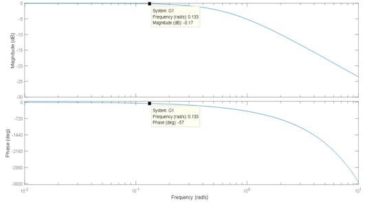
The cut-off frequency is obtained from the magnitude plot of the transfer functions where the magnitude of the response is less than or equal to 1, and the phase margin is in the specified value. The sample for calculating the cut-off frequency and the phase margin are shown in Fig. 1.
The iso-damping property of the system is obtained by differentiating the plant with respect to gain cross-over frequency. By obtaining all these three values and substituting them in the equations 1-3, an unsolved non-linear equation will be obtained.
2.3. Satin bowerbird optimization
The unsolved nonlinear equations are solved by using the SBO algorithm to obtain the fractional order controller coefficients. These coefficients are used for the further process to get the tuned response of the system. The Eq. (1) is used as an objective function to determine the value of the coefficient. The steps in Satin Bowerbird algorithm by [24] is taken as basic idea for this paper:
• Random bower generation,
• The probability of each bower,
• Elitism,
• Position updating,
• Mutation,
• Best result obtained from all bower positions.
Fig. 1Cut-off frequency and phase margin of transfer function
2.3.1. Random bower generation
In this, the population of bowerbirds is initialized based on the number of the population described as per the process needs. The values of bowerbirds are based on the lower bound and upper bound. In this paper, the number of population is 50, and the lower bound of controller coefficients is [0 0 0], and the upper bound is [100 100 2]. The value should lie between 0 and 2. Hence, 2 is selected as the upper bound. The position of bowerbirds is initialized by the Roulette wheel Selection method.
2.3.2. Probability of each bower:
The chances of getting the best bower are estimated in this step through the cost function value of each bower based on the following Eq. (4):
where is the cost function of the problem, here is the Eq. (4), is the total number of population.
2.3.3. Elitism
Elitism is the process of finding the best solution at each stage of the optimization process. At each iteration, the position of bowerbird will vary hence the fitness value for the bower will also vary. Hence, in this process, a variable called elite which stores the best bower values in it is set. This value produces the highest fitness function compared to the other bower. The elite will vary for each iteration, and, at the final iteration, the best bower position is obtained from this elite function.
2.3.4. Position updating
The bower position is updated for each iteration based on the three parameters: 1. Attraction power of the bower; 2. Elite Positions; 3. Roulette wheel procedure for calculating . The attraction power of the bower denotes how likely that the particular bower can be elected as elite function. It is represented by :
where the greatest step size has the value of 0.94 and denotes the chance of best solution of bower obtained by Eq. (4). The position of the bower is calculated by:
2.3.5. SBO mutation
The mutation of SBO refers that the stronger bower may suppress the weaker bower by stealing its values or even the weaker bower may not be considered. Due to this also, the bower position will vary. This is calculated by using the normal distribution (N) of the average value of old position and variance of the space width between the upper and lower limit.
2.3.6. Motivated output result
At each iteration, the population is calculated before and after the changes. The best value is obtained by sorting the population based on a cost function. The whole process will be terminated only when it satisfies the cost function condition till that the steps will be repeated.
2.3.6.1. Pseudocode for SBO algorithm
Pseudocode for SBO algorithm:
Initialize maximum iteration = 100; 50 0.94 and 0.02 [0 0 0]; [100 100 2];
Output as , , ;
Assign position for bowers randomly;
Assign cost function as Eq. (1);
Calculate elite by assuming value;
While (condition is not satisfied);
Calculate using Eq. (4);
For (all bower);
For (all elements of bower);
Update bower positions using roulette wheel based on mutation and Eq. (5), (6).
End for.
End for.
Calculate cost function value for all bowers;
Sort and obtain the best compared value with elite;
Output= elite;
End while;
Return Output.
From the above algorithm, the FOPI coefficients are calculated for each process which is saved for the simulation purpose. Table 3 shows FO controller coefficients.
Performance of controllers is carried out with a new algorithm where the comparisons of methods are presented, and its damping oscillations are reduced and applied to proposed low power converters. The TPC, which used a PMSM motor drive with a single stage conversion system, is illustrated in Fig. 6. The proposed system consists of ampere-hour unit powered MOBB converter, B4-Inverter fed PMSM motor and ampere-hour unit powered bidirectional converter which function as a backup supply for the load operating under demand condition. The proposed converter consists two diodes (, ), swithes (, ), inductor , Capacitor . The proposed converter topology of operation is shown in Fig. 1.
Table 3FO controller coefficients
Transfer functions | Nelder-Mead | SBO tuning | ||||
G1 | 1.1904 | 0.74787 | 1.3323 | 11.0003 | 0.7479 | 1.9032 |
G2 | 0.078619 | 0.28559 | 0.52694 | 1.0140 | 0.4363 | 1.3305 |
G3 | 100 | 100 | 0.87071 | 83 | 25.1230 | 1.1263 |
G4 | 100 | 100 | 0.8675 | 100 | 100 | 1.6548 |
G5 | 15.17169 | 2.1875 | 0.062772 | 15.17169 | 2.1875 | 0.2725 |
2.4. Proposed converter: modes of operation
Mode 0: When the switch () is in “ON” condition, and the switch () is in “OFF” condition, current in inductance () drops (discharging). As a result, the intermediary capacitor () gets (charging) energy from an input inductor (). Consequently, voltage across the intermediary capacitor boosts as given in Fig. 2(a).
Mode 1: When the switch () is in “ON” condition, current in supply voltage drops (discharging). Consequently, the energy is transmitted to the inductance () (charging). Therefore, voltage across the intermediary capacitor () boosts as given in Fig. 2(a). Simultaneously, current in the capacitor () and supply current () drop (discharging). As a result, the energy is transmitted to the capacitor () (charging) with the help of diode . Consequently, voltage across the intermediary capacitor boosts as given in Fig. 2(b).
Mode 2: When switches and are in “OFF” condition, current in inductance drops (discharging). As a result, the intermediary capacitor () gets (charging) energy from input inductor () with the help the diode Fig. 2(c).
Closed loop system of proposed converter depends on PID controller. The PID controller examines to the desired set point through calculation for regulated voltage and output obtained in the desired level. Finally, it controls the process. PID controller algorithm can be run by the obtained Eq. (7):
where means: is set voltage – actual voltage.
The desired output voltage is obtained by the control strategy of MOBB converter as shown in the Fig. 3, The value is 0.2. The switching frequency value is 5 kHz; 10 kHz, where , 0.2 , 4 represents the controller gain and generates saw-tooth signal (), that generates the gate signals (, ), to MOBB converter switches (, ).The output voltage equation is given by:
Conduction losses of switch: :
Switch losses during conduction is expressed in Eq. (10):
At instance of switching current () is derived from Eq. (12):
Fig. 2a), b) [23-24], c) Modes of operation, d) block diagram of closed loop system. Summary: Operation Mode 0: Capacitor C1 charging from inductance L1, Mode 1: Inductance L1 charging from PV panel and voltage balancing capacitor C02 charging from intermediary capacitor C1, Mode 2: Voltage balancing capacitor C01 charging from inductance L1
![a), b) [23-24], c) Modes of operation, d) block diagram of closed loop system. Summary: Operation Mode 0: Capacitor C1 charging from inductance L1, Mode 1: Inductance L1 charging from PV panel and voltage balancing capacitor C02 charging from intermediary capacitor C1, Mode 2: Voltage balancing capacitor C01 charging from inductance L1](https://static-01.extrica.com/articles/20014/20014-img2.jpg)
a)
![a), b) [23-24], c) Modes of operation, d) block diagram of closed loop system. Summary: Operation Mode 0: Capacitor C1 charging from inductance L1, Mode 1: Inductance L1 charging from PV panel and voltage balancing capacitor C02 charging from intermediary capacitor C1, Mode 2: Voltage balancing capacitor C01 charging from inductance L1](https://static-01.extrica.com/articles/20014/20014-img3.jpg)
b)
![a), b) [23-24], c) Modes of operation, d) block diagram of closed loop system. Summary: Operation Mode 0: Capacitor C1 charging from inductance L1, Mode 1: Inductance L1 charging from PV panel and voltage balancing capacitor C02 charging from intermediary capacitor C1, Mode 2: Voltage balancing capacitor C01 charging from inductance L1](https://static-01.extrica.com/articles/20014/20014-img4.jpg)
c)
![a), b) [23-24], c) Modes of operation, d) block diagram of closed loop system. Summary: Operation Mode 0: Capacitor C1 charging from inductance L1, Mode 1: Inductance L1 charging from PV panel and voltage balancing capacitor C02 charging from intermediary capacitor C1, Mode 2: Voltage balancing capacitor C01 charging from inductance L1](https://static-01.extrica.com/articles/20014/20014-img5.jpg)
d)
Fig. 3Control of MOBB converter [24]
![Control of MOBB converter [24]](https://static-01.extrica.com/articles/20014/20014-img6.jpg)
Oscillation of power devices current () is given as per Eq. (13):
The power controlled devices losses are obtained from the Eq. (14) depending on the values of Fig. 4:
Fig. 4Open loop waveform during switch (S1,2) conduction [24]
![Open loop waveform during switch (S1,2) conduction [24]](https://static-01.extrica.com/articles/20014/20014-img7.jpg)
2.4.1. On and off losses of switch () during starting condition
Power controlled devices on and off losses are derived from the Eq. (16):
2.4.2. Inductor losses ()
The converter inductor losses are given by Eq. (17):
Fig. 5Open waveform during the conduction of inductor (L1) [23]
![Open waveform during the conduction of inductor (L1) [23]](https://static-01.extrica.com/articles/20014/20014-img8.jpg)
2.4.3. Voltage-current losses of converter
The total power losses of the converter using PID controller are given by Eq. (21):
where is output power of MOBB converter (39 W) and refers power losses.
A proposed TPC converter for the implementation of PMSM motor drive MOBB converter using four switch inverters in a single standalone are shown in Fig. 6.
Fig. 6Proposed MOBB converter fed PMSM drive system using four switch inverter in a single standalone system
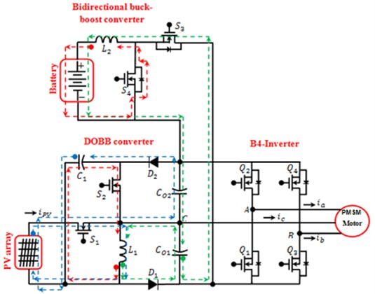
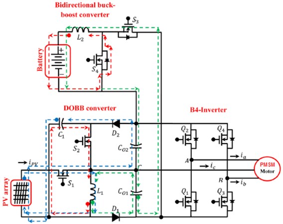
Power device present in converter at the proposed work is to extract the radiation from solar panel using the P&O MPPT algorithm. On the contrary, the regulation of the total output voltage to the required value is made by the power sharing switch () present in the MOBB converter. In addition, when the generated energy is sufficient to drive the PMSM motor, the excess energy is utilized for charging the battery. When the power switch () is turned on, the inductor L1 stores the energy, and thereafter there is an energy flow from the PV module to the battery. If the energy that is generated at the PV module is not adequate to drive the PMSM motor, then the power system acts as a boost converter, making the energy transfer from the battery to the PMSM motor. When the switch (s1) is turned on, the inductor () stores the energy from the battery, and, if the switch s2 is turned off, the energy that is stored in the inductor is transferred to the PMSM motor. The command signals of the switches (, ) are complementary. Proposed MOBB converter fed pmsm drive system using four switch inverter in a single standalone system operates in different power flow modes such as Battery Energizing unit (BEU), Solar Module (SM) and Battery Deenergizing unit (BDU).
2.4.4. Battery energizing unit (BEU)
Operation mode A.
Meanwhile at Operation mode A controlled device gets triggered controlled devices (, and ) are not triggered. Input inductor () destores electrons, the current () reduces, in between capacitor () gets boosted.
Operation mode B.
Meanwhile at Operation mode B controlled device is triggered “ON”, then controlled devices (, and ) not triggered. Meanwhile () stores energy from the input source, and electrons across inductor () increases, then in between capacitor () and solar unit act as series connected sources and start destores electrons to output () through the diode ().
Operation mode C.
Meanwhile at Operation mode C controlled device is triggered, controlled devices (, and ) not triggered. Ampere-hour module gets energy from source () current through the diode (), and ampere hour module highly boosted ().
Operation mode D.
Meanwhile at Operation mode D controlled devices and are triggered, the controlled devices ( and ) are not triggered. The in between capacitor stores energy at inductor () current, then ampere hour module gets stored the value from inductor () current via the diode ().
Fig. 7Proposed MOBB converter fed PMSM drive system using four switch inverter in a single standalone system at BEU mode
2.4.5. Solar module (SM)
Operation mode E.
Meanwhile at Operation mode E controlled device gets triggered controlled devices (, and ) are not triggered. Input inductor () destores electrons, the current () reduces, in between capacitor () gets boosted.
Operation mode F.
Meanwhile at Operation mode F controlled device is triggered, the input inductance (L1) gets charging from the input DC supply. Thus, the current in input inductance increases. Simultaneously, the current in the intermediate capacitor () and input supply act as series sources, and the energy of intermediate capacitor is transferred to the output capacitor ().
Operation mode G.
Meanwhile at Operation mode G controlled device and and are not triggered, the electrons in () destores the energy to the output capacitor through the diode.
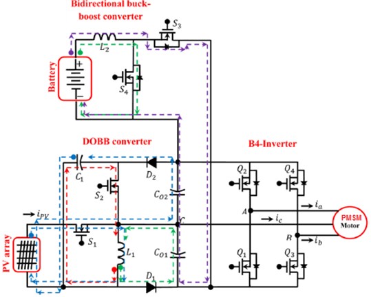
2.4.6. Battery deenergizing unit (BDU)
Operation mode H.
Meanwhile at Operation mode H Controlled device is triggered, so , and not triggered. Input () destores the energy, meanwhile electrons () decreases, in between capacitor () energizes.
Operation mode I.
Meanwhile at Operation mode I Controlled device is triggered, controlled devices , and are not triggered. stores energy from the input source, and electrons across inductor () increases, then in between capacitor () and solar unit act as series connected sources and start deliver current electrons to output () through the diode ().
Operation mode J.
Meanwhile at Operation mode J controlled devices, are triggered then controlled devices and are not triggered. Input () stores from source, and electrons from () energizes, ampere hour module destores to input () through diode (). Then inbetween capacitor and input source destores the energy to the output capacitor .
Fig. 8Proposed MOBB converter fed PMSM drive system using four switch inverter in a single standalone system at BDU
3. Results and discussions
The following graph shows the outputs for the different-order integrator process with dead time transfer functions for load disturbance which is the regulatory response. The regulatory system is the system in which the response will get settled by itself in the set point without any external influence when the disturbance is given. The Error performance values for actual coefficients are shown in Table 4.
Table 4Error performance values for actual coefficients
Transfer functions | Nelder-mead | SBO tuning | ||||
ISE | IAE | ITAE | ISE | IAE | ITAE | |
G1 | 6.248 | 33.52 | 3139 | 0.7091 | 4.632 | 168.3 |
G2 | 35.61 | 64.6 | 5340 | – | – | – |
G3 | 0.004961 | 0.02911 | 1.629 | 0.006052 | 0.02117 | 0.7052 |
G4 | 0.004978 | 0.05233 | 3.961 | 0.005161 | 0.03506 | 0.4864 |
G5 | – | – | – | – | – | – |
The robustness of controller is analyzed by calculating the IAE, ISE and ITAE. These values are calculated for both positive and negative mismatch of the controller for both the existing and proposed method. The positive mismatch denotes 10 % increase of controller coefficient values, and the negative mismatch denotes decrease of 10 % from its values. It is shown in Tables 5, 6.
Table 5Positive mismatch of controller values
Transfer functions | Nelder-mead | SBO tuning | ||||
ISE | IAE | ITAE | ISE | IAE | ITAE | |
G1 | 0.8883 | 2.179 | 37.42 | 2.582 | 19.53 | 2084 |
G2 | – | – | – | – | – | – |
G3 | 0.004535 | 0.02282 | 1.059 | 0.005507 | 0.02218 | 0.6247 |
G4 | 0.004547 | 0.03358 | 2.458 | 0.004814 | 0.05963 | 0.9328 |
G5 | – | – | – | – | – | – |
Table 6Negative mismatch of controller values
Transfer functions | Nelder-mead | SBO tuning | ||||
ISE | IAE | ITAE | ISE | IAE | ITAE | |
G1 | 0.9913 | 2.585 | 42.15 | 0.633 | 2.949 | 57.66 |
G2 | – | – | – | – | – | – |
G3 | 0.005455 | 0.04194 | 2.751 | 0.006717 | 0.02157 | 0.8568 |
G4 | 0.005502 | 0.08069 | 6.35 | 0.005678 | 0.02817 | 0.3776 |
G5 | – | – | – | – | – | – |
3.1. Disturbance rejection property
The system is disturbed by a disturbance 0.1 at 200. Then the system is analyzed by the rise time, settling time and overshoot values. For a good controller, the settling time and overshoot value should be less. The performance of the proposed method is compared with the Nelder-Mead and shown in Table 7.
The Table 8 shows the simulation specifications. The characteristics of a 80 W solar module are simulated using the MATLAB tool based on the equivalent circuit model. The simulation of the controller is listed separately in order to denote the looping and the unit time constant of the controller.
Table 7Comparison of disturbance rejection properties
Transfer functions | Nelder-mead | SBO tuning | ||||
Rise time | Settling time | Overshoot | Rise time | Settling | Overshoot | |
Time | ||||||
G1 | – | – | – | 11.7799 | 300.8208 | 49.9781 |
G2 | 23.1994 | 980.1611 | 59.0062 | 30.0543 | 1101.0 | 0 |
G3 | 14.8177 | 25.4632 | 0.7828 | 19.9530 | 31.7672 | 0.1219 |
G4 | 15.0689 | 25.8720 | 0.8513 | 18.4335 | 29.8387 | 0.7560 |
G5 | – | – | – | – | – | – |
Fig. 9Response of G1 FO-PI controlled process
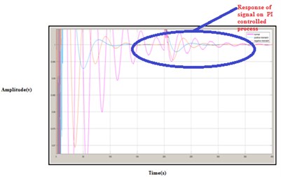
Fig. 10Response of G2 FO-PI controlled process
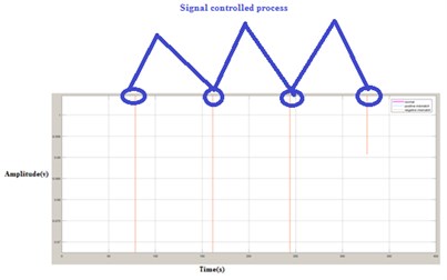
Fig. 11Response of G3 FO-PI controlled process
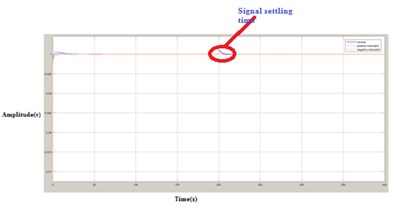
Fig. 12Response of G4 FO-PI controlled process
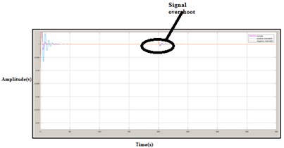
Table 8Simulation specifications for proposed converter using PI controller system
S. No. | Objects | Values |
1 | Solar module voltage | 22.17 V |
2 | Solar module current | 1.02 A |
3 | Solar module power | 73.7 W |
4 | Proposed converter output voltage | 47 V |
5 | Proposed converter output power | 39.4 W |
6 | Rated PMSM motor power (Torque = 0.128 Nm, Speed = 3000 Rpm, DC link voltage = 26 V, number of poles = 8) | 39 W |
7 | Nominal power of battery (Nominal voltage = 10 V, Nominal current = 7.2 A/h) | 80 W/h |
3.2. Simulation output voltage control Asymmetrical for proposed converter
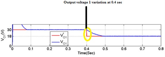
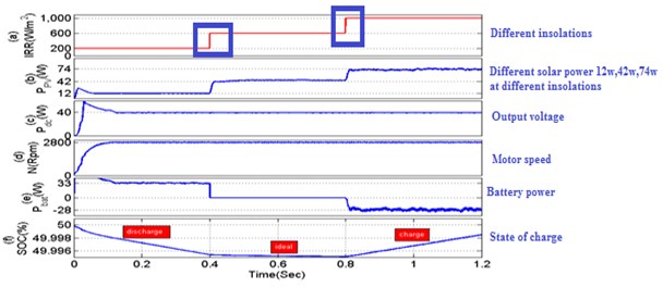
To verify the asymmetrical validation of proposed converter, source input fed is ( 18 V) as determined in Fig. 13. Similarly, resistance ( 28.8 ) are used load, asymmetrical condition. The output voltages of the proposed converter are desired to be regulated on ( 30 V and 18 V) from 0 to 0.4 Sec. The total powers and are drawn under asymmetrical are stated in the Fig. 13(a)-(d). Fig. 13(e), () total output power () denotes output voltage, powers. As seen from this figure, voltage and power are tracked with the reference’s values ( 48 V and 42.5 W).
The following Table 9 shows the values for the rise time, peak time, settling time and peak overshoot of the transfer function 1 for the load disturbance. These methods do not show the good response for few methods since it has little high time delay.
Table 9Comparison of various parameters
Methods | (Rise time) (ms) | (Peak time) (ms) | (Settling time) (ms) | Peak Overshoot |
Process reaction curve method | 15 | 34 | 150 | 0.35 |
Ziegler Nichols | 7 | 11 | 80 | 1.4 |
Robust method | 9 | 15 | inf | 175 |
Ultimate cycle method | 6 | 29 | 150 | 0.75 |
Direct synthesis method | 20 | 12 | 45 | 0.15 |
IMC method | 7 | 11 | inf | 1.75 |
Tyreus-Luyben | 9 | 125105 | 0.1523 | 4 |
Fig. 13Output voltage variations
a)

b)

c)

d)

e)
f)
3.3. Experimental analysis of transfer function using TPC and b4-inverter fed PMSM motor driver
Experimental Analysis of Transfer Function Using TPC And B4-Inverter Fed PMSM Motor Driver is conducted for examining the enhanced TPC and B4-Inverter fed PMSM motor drive. The hardware of transfer function output to TPC and B4-Inverter fed PMSM motor drive is presented in Fig. 15.
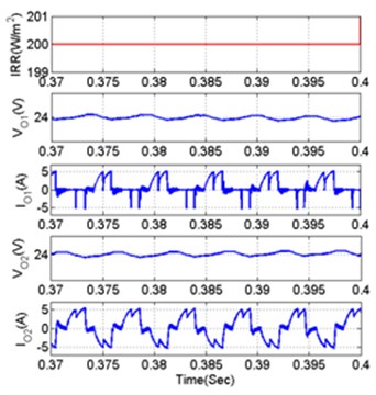
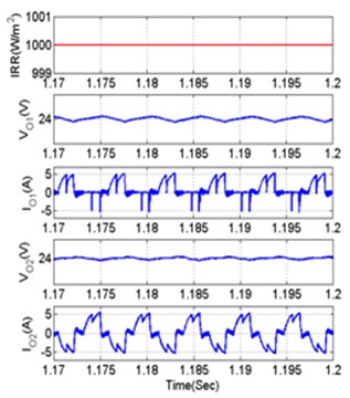
Fig. 14Performance of MOBB converter under symmetrical voltage and battery insolation condition TPC parameters under different insolation condition a) 200 W/m2, b) 1000 W/m2
a)
b)
Fig. 15Experimental illustration for TPC and B4-Inverterfed PMSM motor drive
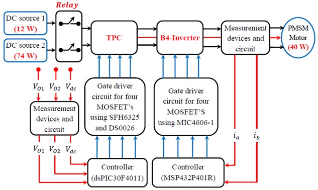
The hardware TPC and B4-Inverter fed PMSM motor drive consists of a 16-Bit digital signal Peripheral Interface Controller (DSPIC30F4011) for TPC control, a 32-Bit Mixed-Signal Microcontroller (MSP432P401R) for B4-Inverter control, a gate driver circuit for TPC and B4-Inverter MOSFET are employed. Table 10 shows the hardware specification.
Table 10Hardware specification
S. No. | Name of the equipment | RANGE |
1 | Battery | 12V/4.7AH |
2 | Step down transformer | 230V/12V |
3 | Step down transformer | 230V/5V |
4 | MOSFET | SFH6325 |
5 | PMSM motor | 220 V, 100 mA, 60 rpm |
3.4. Experimental results of output voltage
The below Fig. 16 is output voltage waveform. These PWM pulses are generated by the B4 inverter which these signals are fed through the PMSM motor drive.
Fig. 16Output voltage C01 at 1000 w/m2: a) experimental, b) simulation

a)

b)
3.5. Experimental results of PWM pulses of and
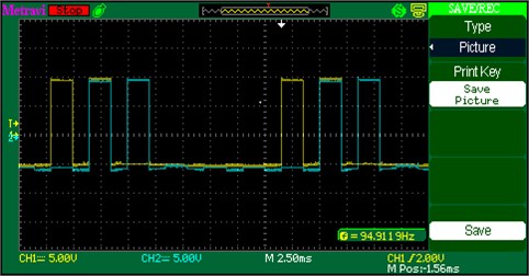
The below Fig. 17 is the output waveform of PWM Pulses across the switches and . These PWM pulses are generated by B4 inverter which these signals are fed through the PMSM motor drive.
Fig. 17Output voltage waveform of PWM pulses of S1 and S4
3.6. Experimental results of DC-DC converter output voltage
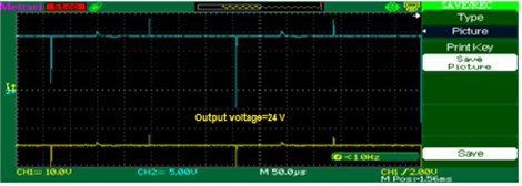
Fig. 18 represents proposed MOBB converter generates the voltage of about 24 V, during solar insolation of 800 W/m2.
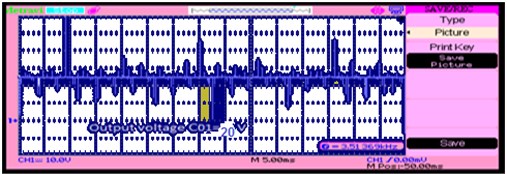
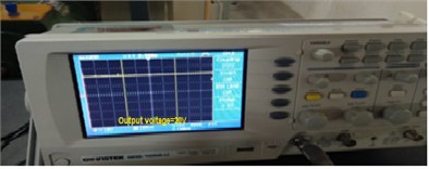
Fig. 19 represents proposed MOBB converter generates the voltage of about 20 V, during solar insolation of 600 W/m2.
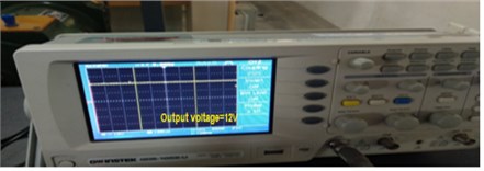
Fig. 20 represents proposed MOBB converter generates the voltage of about 12 V, during solar insolation of 200 W/m2. Based on the new technical proposed on PI controller on the power devices the Performance Comparison of the conventional and proposed MOBB converters with various objects is shown in Table 11.
3.7. Prototype experimental setup
Experimental setup of enhanced three-port converter fed PMSM motor are shown in Fig. 21. When the PMSM is driven by different switching frequency inverters, the acoustic noise spectrum has highly concentrated harmonic energy near the switching frequency and its multiples. The proposed research involves triangular, saw-tooth periodic switching frequency modulation patterns to transfer discrete power spectrum to much wider frequency ranges, so as to limit the acoustic noise at a low cost. To reduce the vibration under different switching frequencies on the PMSM motor, the motor shall be optimized. Then, by using controller techniques, the optimization is made on the motor. It is shown in Figs. 22 and 23.
Table 11Performance comparison of the conventional and proposed MOBB converter with various objects
Substances | Various two output converters | |||
Converter accessible by Sathish Kumar et al. (2017) [25] | Converter accessible by Senthilkumar et al. (2018) [26] | Proposed converter for DTC | ||
Switch count total | 2 | 2 | 2 | |
Total number of diodes count total | 2 | 3 | 2 | |
Total number of capacitors count total | 2 | 2 | 3 | |
Total number of Inductors count total | 1 | 1 | 1 | |
Total number of components count total | 7 | 9 | 8 | |
Conversion | Buck | Buck-Boost | Buck-Boost | |
Switching states convolution | Easy | multifarious | Easy | |
Vibration measurement at PMSM motor using improved DC-DC converter | 87.1 % | 87.1 % | 92.28 % | |
Converter presented by Sathishkumar et al. (2017) [25] | ||||
Power controlled devices conduction stage | Output capacitors stage | |||
– | ||||
1 | 0 | – | Stored | De-stored |
0 | 1 | – | De-Stored | Stored |
0 | 0 | – | De-Stored | De-stored |
Converter presented by Senthilkumar et al. (2018) [26] | ||||
Switching states | States of output capacitors | |||
1 | 0 | 0 | Stored | De-Stored |
1 | 0 | 1 | Stored | stored |
0 | 0 | 1 | De-stored | stored |
0 | 0 | 1 | De-Stored | stored |
0 | 0 | 0 | De-Stored | De-Stored |
1 | 1 | 0 | stored | stored |
Proposed converter for DTC | ||||
Switching states | States of output capacitors | |||
– | ||||
0 | 0 | – | De-stored | De-stored |
0 | 1 | – | Stored | De-stored |
1 | 0 | – | Stored | De-stored |
Fig. 18Output voltage C02: a) experimental, b) simulation, c) chart at 800 W/m2
a)

b)

c)
Fig. 19Output voltage waveform of DC-DC: a), b) experimental, c) simulation of converter, d) chart at 600 W/m2
a)
b)

c)

d)
Fig. 20a) Experimental output voltage waveform of DC-DC converter experimental, b) chart at 200 W/m2
a)

b)
Fig. 21Experimental setup of enhanced three-port converter fed PMSM motor
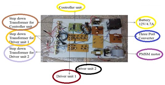
Fig. 22Experimental vibration of motor without optimization
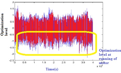
Fig. 23Experimental vibration of motor with optimization
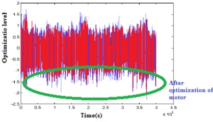
Table 12Comparison parameters on vibrations on PMSM
Substances | Vibration measurement by Lakshmikanth et al. (2017) [27] | TPC for proposed converter fed PMSM motor vibration measurement |
Switching frequency | 134 Hz | 125 Hz |
Switching states convolution | easy | Easy |
Motor optimization for industrial applications | Moderate | Easy |
Switching pulses | Moderate | Easy |
Time (s) | 20 | 18 |
Conversion | Buck | Buck-Boost |
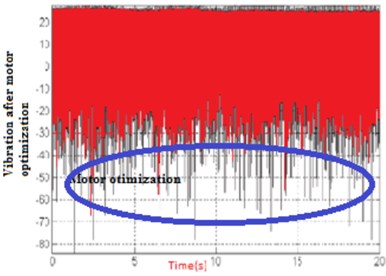
To reduce the vibration under different switching pulses on the PMSM motor, the motor shall be optimized. Then, by using controller techniques, the optimization is made on the motor. It is shown in Figs. 24 and 25. The various comparison parameters on vibrations are shown in Table 12.
Fig. 24Experimental vibration of motor during startup
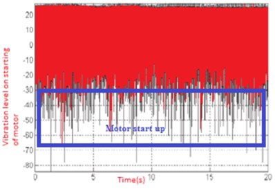
Fig. 25Experimental vibration of motor after reduction
4. Conclusions
An analysis is made for four different integrator time delay transfer functions for different time delays and shows the disturbance rejection and system performance for the different PID controllers for load disturbance, it shows good performance for the transfer functions with the delay less than 2. Compared to other methods, the proposed method results are good for the pure integrator process transfer function with the time delay 5. Thus, the pure integrator process having small time delay shows better response. Dead time compensators can be used for the process with a large time delay so that better response can be obtained. A simulation of fractional second order function, a Buck-Boost converter is designed, and its concert is analyzed for various functioning factor conditions. Proposed converter works in asymmetrical condition for harvesting the battery life. Similarly, two output capability is appropriated for B4-inverter which reduces the cost of this proposed system probably. The design along with a reduced number of components minimizes the current conduction losses and assists in increasing the service life of the switches. The Controller shows a significant part in controlling the system output based on the output need. In such a situation the controller has to be tuned one and also the operation of the controller should be an easy one. Hence, this paper proposed an SBO based tuned FOPI for a different process. The FOPI is chosen over the traditional PI because the fractional order requires only less no of computation when controllers are increased. For the tuning purpose, the SBO algorithm is employed because the position initialization of the bowers is based on the probability of best bower and mutation step. While in the Nelder-Mead of tuning the positions are randomly initialized which affects the tuning process of the controller. Based on the performance evaluation also, the proposed method outperforms the Nelder-Mead and produced the best tuning of FOPI controller for different transfer functions. The SBO tuning produces less overshoot as compared to the existing method. The proposed technique produces less variations in positive and negative mismatch. The values indicated in “-” denotes that the result produces the larger value which is not suitable for the tuning. The tuning of parameters based on SBO technique is suitable for the input without delay functions. In future, the SBO and Nelder-Mead tuning has to improve to produce the best results for delayed unit not only based on the stable region of the output as in the other methods.
References
-
Blaabjerg F., Freysson S., Hansen H. H., Hansen S. New optimized space-vector modulation strategy for component-minimized voltage source inverter. IEEE Transactions of Power Electronics, Vol. 12, Issue 4, 1997, p. 704-714.
-
El Badsi B., Bouzidi B., Masmoudi A. DTC scheme for a four-switch inverter fed induction motor emulating the six-switch inverter operation. IEEE Transaction of Power Electronics, Vol. 28, Issue 7, 2013, p. 3528-3538.
-
El Badsi B. Six-switch inverter emulation based DTC strategy dedicated to three-switch inverter-fed induction motor drives. Computational Mathematics Electrical Electronics Engineering, Vol. 32, Issue 1, 2013, p. 289-301.
-
El Badsi B., Bouzidi B., Masmoudi A. Bus-clamPIng-based DTC: Attempt to reduce harmonic distortion and switching losses. IEEE Transactions of Industrial Electronics, Vol. 60, Issue 3, 2013, p. 873-884.
-
Fang J., Zhou X., Liu G. Instantaneous torque control of small inductance brushless DC motor. IEEE Transactions of Power Electronics, Vol. 27, Issue 12, 2012, p. 4952-4964.
-
Ellis M. W., Von Spakovsky M. R., Nelson D. J. Fuel cell systems: efficient, flexible energy conversion for the 21 st century. Proceedings of the IEEE, Vol. 89, Issue 12, 2001, p. 1808-1818.
-
Gao F., Blunier B., Simoes M. G., Miraoui A. PEM fuel cell stack modeling for real-time emulation in hardware-in-the-loop application. IEEE Transactions on Energy Conversion, Vol. 26, Issue 1, 2011, p. 184-194.
-
Jidin A. B., Idris N. R. B. N., Yatim A. H. B. M., Elbuluk M. E., Sutikno T. Wide-speed high torque capability utilizing overmodulation strategy in DTC of induction machines with constant switching frequency controller. IEEE Transaction of Power Electronics, Vol. 27, Issue 5, 2012, p. 2566-2575.
-
Joice C. S., Paranjothi S. R., Kumar V. J. S. Digital control strategy for four quadrant operation of three phase BLDC motor with load variations. IEEE Transactions on Industrial Applications, Vol. 9, Issue 2, 2013, p. 974-982.
-
Kang S. J., Sul S. K. Direct torque control of brushless DC motor with non-ideal trapezoidal back-EMF. IEEE Transaction of Power Electronics, Vol. 10, Issue 6, 1995, p. 796-802.
-
Kumar R., Singh B. BLDC motor-driven solar PV array-fed water pumping system employing zeta converter. IEEE Transactions on Industry Applications, Vol. 52, Issue 3, 2016, p. 2315-2322.
-
Kumar R., Singh B. Solar PV powered BLDC motor drive for water pumping using Cuk converter. IET Electric Power Applications, Vol. 11, Issue 2, 2017, p. 222-232.
-
Liu Y., Zhu Z. Q., Howe D. Direct torque control of brushless DC drives with reduced torque ripple. IEEE Transaction of Industrial Applications, Vol. 41, Issue 2, 2005, p. 599-608.
-
Sathishkumar S., Meenakumari R., Jobanarubi E., Anitta P. J. S., Ravikumar P. Microcontroller Based BLDC Motor Drive for Commercial Applications. Power Electronics and Renewable Energy Systems, Lecture Notes in Electrical Engineering, Springer, New Delhi, Vol. 326, 2015, p. 829-841.
-
Shanmugam S., Ramachandran M., Kanagaraj K., Loganathan A. Sensorless control of four-switch inverter for brushless DC motor drive and its simulation. Circuits and Systems, Vol. 7, Issue 6, 2016, p. 726-734.
-
Stirban A., Boldea I., Andreescu G. Motion-sensorless control of BLDC-PM motor with offline FEM-information-assisted position and speed observer. IEEE Transactions of Industrial Applications, Vol. 48, Issue 6, 2012, p. 1950-1958.
-
Sung P. J., Han W. P., Man L. H., Harashima F. New approach for minimum-torque-ripple maximum- efficiency control of BLDC motor. IEEE Transaction of Industrial Electronics, Vol. 47, Issue 1, 2000, p. 109-114.
-
Taheri, Rahmati A., Kaboli S. Efficiency improvement in DTC of six-phase induction machine by adaptive gradient descent of flux. IEEE Transaction of Power Electronics, Vol. 27, Issue 3, 2012, p. 1552-1562.
-
Boora A., Zare F., Ghosh A. Multi-output buck-boost converter with enhanced dynamic response to load and input voltage changes. IET Power Electronics, Vol. 4, Issue 2, 2011, p. 194-208.
-
Boora A., Nami A., Zare F., Ghosh A., Blaabjerg F. Voltage sharing converter to supply single-Phase asymmetrical four-level diode-clamped inverter with high power factor loads. IEEE Transactions on Power Electronics, Vol. 25, Issue 10, 2010, p. 2507-2520.
-
Sigurd Skogestad Probably the best simple PID tuning rules in the world. AIChE Annual Meeting, 2001.
-
De Keyser R., Muresan C. I., Ionescu C. M. A novel auto-tuning method for Fractional order PI/PD controllers. ISA Transactions, Vol. 62, 2016, p. 268-275.
-
Bequette B. W. Process control- Modeling, Design and Simulation. Prentice Hall, 2003.
-
Moosavi S. H. S., Bardsiri V. K. Satin bowerbird optimizer: a new optimization algorithm to optimize ANFIS for software development effort estimation. Engineering Applications of Artificial Intelligence, Vol. 60, 2017, p. 1-15.
-
Shanmugam Sathish Kumar, Arumugam Senthilkumar Design and implementation of DC source fed improved dual-output buck-boost converter for agricultural and industrial applications Journal of Vibroengineering, Vol. 19, Issue 8, 2018, p. 6233-6454.
-
Arumugam Senthilkumar, Govindaraj Vijayakumar, Shanmugam Sathish Kumar Solar photovoltaic array fed brushless DC motor drive using sensorless technique for reducing vibration with enhanced DC-DC converter. Journal of Vibroengineering, Vol. 20, Issue 6, 2018, p. 2515-2538.
-
Lakshmikanth S., Natraj K. R., Rekha K. R. Noise and vibration reduction in permanent magnet synchronous motors – a review. International Journal of Electrical and Computer Engineering (IJECE), Vol. 2, Issue 3, 2017, p. 405-416.
