Abstract
This paper presents a new grid-connected control strategy based on a new type of Z-source inverter. For this Z-source inverter, a coupled inductor is used to displace the inductor connected to the positive of the power supply in traditional Z-source topology and its position relative to the three-phase inverter bridge has changed. In contrast with traditional Z-source inverter, it can achieve higher voltage gain, lower capacitor voltage stress during steady state and suppress inrush current at startup. Last, it is modeled in two-phase static frame and then a grid-connected power loop and a capacitor voltage loop are used to realize it to connect grid. Simulation results show that by this new grid-connected strategy, this Z-source inverter can reach its grid connection with high power factor and the system can work in good stability, strong robustness and dynamic performance.
1. Introduction
Z-source inverter makes the shoot-through phenomenon of the upper and lower devices of each phase leg become a normal state by using its unique impedance network while conducting its work [1, 2] and also avoids the distortion of output voltage waveform with the insertion of dead time. So it can overcome the shortcomings of traditional voltage and current source inverters [3, 4]. However, traditional -source inverter also remains many deficiencies [5-8]: Inrush current which is easy to damage the devices of three-phase inverter bridge at startup. High capacitor voltage stress on impedance network during steady state, therefore large volume of capacitors is required and then the cost increases for this inverter. In addition, due to the shoot-through zero vectors were replaced part of traditional zero vectors, so the circle synthetic generated by SVPWM is not so smooth and then quality of AC output voltage is affected. In order to further improve this topology, the scholars have proposed a variety of different Z-source inverter Topologies: a modified Z-source inverter was proposed [9, 10]. It has many advantages with no inrush current at startup and lower capacitor voltage stress during steady state compared to the traditional Z-source inverter, but its boosting capacity has not been improved. It was presented a type of Z-source inverter named switching inductive Z-source inverter in [11], this topology reduces the capacitor voltage stress and upgrades boot capacity, but on account of increasing the number of inductor elements, and thus increase the cost a lot. Last, two types of Z-source inverters called switching inductive quasi Z-source inverter and high gain Z-source inverter were proposed in ref [12, 13]. Although they can improve boost capacity, the capacitor voltage stress is still high during steady state. What’s more, the high gain Z-source inverter forms great inrush current when it starts working and is easy to damage components in the circuit. [14] lists many Z-source topologies, all have different properties, but they master boost capacity through adding shoot-through zero vectors to replace traditional zero vectors, in turn the waveform of output voltage are affected to a certain extent.
Z-source inverter is used to connect to the grid finally. As to the control strategy of grid connection for Z-source inverter, [15] proposed a control strategy named Hysteresis Current Control, it has advantage of simple control to any topologies to realize tracking control, but whether its function can achieve is based on hysteresis width. Due to the parameters complicated setting for hysteresis width, the stability of whole control system cannot be guaranteed. [16] established mathematical mode of three-phase voltage source inverter in frame, PR controllers were adopted to control state variables and LCL filter was included to implement better filtering effect in ac side, but it generates resonance meanwhile. In addition, parameters of PR controllers are hardly to set accurately and then the stability cannot be also guaranteed.
As can be seen from the above analyses, although the Z-source inverters mentioned above overcome some deficiencies of traditional Z-source inverter to some extent, there are still substantial shortcomings. So a new type of Z-source inverter named isolated shoot-through Z-source inverter with Coupled inductor (IST-ZSI-WCI) is proposed in this paper, whose inrush current does not exist, capacitor voltage stress is much lower during steady state, boost capacity is improved a lot. And the separation between shoot-through vector and traditional zero vector can be realized owing to adding the electric electronic component IGBT. It overcomes all deficiencies of Z-sources inverter mentioned above. Last, it is modeled in frame and then a grid-connected power loop and a DC bus voltage loop are used to realize it to connect grid with high power factor, strong robustness, and then the system can work in good stability and dynamic performance. Simulation results show that the above theoretical analyses are correct and verifying the superiority of this novel topology.
2. Isolated shoot-through Z-source inverter with coupled inductor (IST-ZSI-WCI)
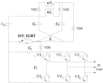
The topology of IST-ZSI-WCI is shown in Fig. 1. It consists of three-phase inverter and Z-source network including capacitors , and inductors , . Especially, a coupled inductor is used to replace one of inductors of traditional Z-source network, and the relative position between Z-source network and three-phase inverter bridge is different from tradition Z-source inverter to suppress inrush current. Its boost capacity is based on the polarity change of primary and secondary winding of coupled inductor and turning on or off diode to implement boost. Whereby, controlled device IGBT is used to individually control the insertion of shoot-through zero vector and achieve separation between shoot-through zero vectors and traditional zero vectors, Capacitor is used to suppress fluctuation of bus voltage due to the insertion of shoot-through zero vector. In order to avoid capacitor discharging through IGBT. So the diode VDS is added to make isolation.
Fig. 1Topology of this novel inverter
2.1. Modulation strategy
Space vector pulse width modulation (space vector pulse width modulation, SVPWM) [15, 16] is selected in this paper. Compared to the modulation strategy of SPWM, it has advantages including higher utilization of DC voltage, lower harmonic content, fast dynamic response and less volatile, etc.
Fig. 2Control theory of SVPWM
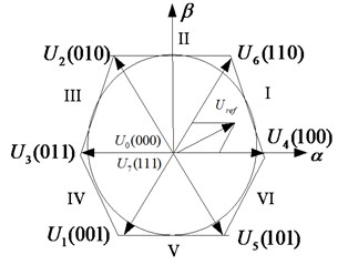
a) The synthesis of space vector
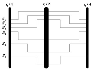
b) Control signal in one switching cycle for Z-source inverter
2.2. Working principle of IST-ZSI-WCI
Assuming that is a shoot-through interval in a switching cycle, is a traditional zero vector state interval in a switching cycle, is an effective vector state interval in a switching cycle. so . Ratio of can be denoted by i.e. shoot-through duty ratio. Similarly, and are non-shoot-through duty ratio, is input DC voltage, is inductor voltage in the Z-source passive network, and are the capacitor voltages in the Z-source network during steady state.
As to the coupled inductor of the novel Z-source network, it is equivalent to a magnetizing inductor and a leakage inductor as well as an ideal transformer whereby, the coupled coefficient of coupled inductor and turns ratio of ideal transformer are respectively as follows:
where, and are respectively the turns of primary winding and secondary winding.
The novel Z-source inverter works in the same state with traditional Source inverter: shoot-through zero vector state, traditional zero vector state, effective vector state. Modulation control of simple boost (SVPWM) is used for this novel Z-source inverter.
Interval 1 (): (Fig. 3(a)). The novel Z-source inverter works in shoot-through zero vector state, the inverter bridge leg is short-circuited, because (1), diode VD1 is in off-state and then the power forms a loop with primary winding of transformer through capacitor , and increases from the minimum value at the same time. So the increase of can be written as:
And the power forms a loop with inductor through capacitor and , thus the increase of inductive current is:
Interval 2 (): (Fig. 3(b)). The novel Z-source inverter works in the traditional zero vector state, three-phase inverter bridge leg is open, primary and secondary e mf polarity of ideal transformer changes, the leakage inductor energy is transferred from VD0 branch (short-circuited this moment) to the capacitor and charges it, the interval of leakage inductor energy releasing to zero can be taken as the interval of working in traditional zero vector state for this novel Z-source inverter. During this period, the changes of current across magnetizing inductor can be stated as:
Fig. 3Equivalent circuit of this novel Z-source inverter indifferent states
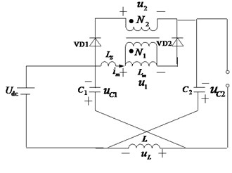
a)
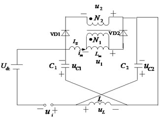
b)
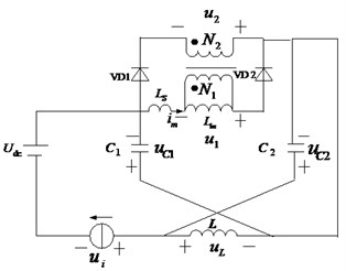
c)
The energy of inductor is transferred from diode VD0 branch (short-circuited this moment) to the capacitor and charges it, reduction of inductive current is:
Due to the expression , Diode VD2 is turn-off and diode VD1 is turn-on at the same time after the release of the energy of leakage inductor . The current of secondary winding is transferred from diode VD0 branch (short-circuited this moment) to capacitor and charges it, accordingly, secondary current decreases. The voltage of magnetizing inductor is and DC voltage across the voltage is . It has been improved.
Interval 3 (): (Fig. 3(c)). The novel Z-source inverter works in an effective vector state; three-phase inverter bridge can be taken as a current source. forms a loop with secondary winding of transformer through original VD0 branch (short-circuited this moment) and voltage of magnetizing inductor is at this point. Current across magnetizing inductor is expressed as:
The current across inductor flows to capacitor and charges it, Reduction of inductive current is:
2.3. Boost property of the novel Z-source inverter
According to the volt-second balance theorem of inductor voltage, average voltage across inductor is zero over a time period , so we have:
They can be also drawn from the above two formulas:
where, is the duty ratio. It also can be regarded as the duty ratio for energy-releasing of the leakage inductor.
The analysis shows that the peak DC voltage across the inverter is:
Boost factor of the novel Z-source inverter is , for the same shoot-through duty ratio, when coupled inductor is fully coupled, boost factor is the highest. So when 1, 0, the highest boost factor can be obtained, the simplified expression is derived for the boost factor:
2.4. Design of coupled inductor for the novel Z source inverter
The expression of coupled inductor for this novel Z-source inverter is [17]:
where , , is the mutual coupled inductor.
The inductor and capacitor in passive Z-source network are designed by their suppression of higher ripple current of inductor and higher ripple voltage of capacitor during steady state:
where, % and % are respectively the percentage of the ripple current of inductor and ripple voltage of capacitor, is the average value of current flowing through the network, is the frequency of switch, is the average value of two pieces of capacitor in the network in steady state.
Traditional Z-source inverter [18, 19] is used as a object to compare with this Z-source inverter in properties.
Capacitor voltage and the peak DC voltage across the inverter during steady state of traditional Z-source inverter can be obtained by volt-second theorem of the voltage of inductance. Expressions are shown as follows:
Assuming coupled coefficient of coupling inductor 1, turns ratio of ideal transformer 2 and then comparison between traditional Z-source inverter and novel Z-source inverter in their capacitor voltage and boost factor in steady state are relatively as follows.
Fig. 4Characteristic contrast of two kinds of Z-Source inverter
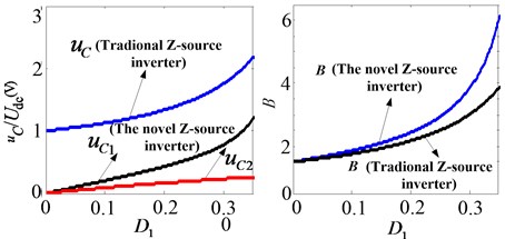
It can be seen from the simulation that in the same shoot-through duty cycle, compared with traditional Z-source inverter for their capacitor voltage and boot factor, the capacitance voltage of novel Z-source inverter is much lower in steady state and its boost factor is much higher.
3. Control of Grid-connected IST-ZSI-WCI
IST-ZSI-WCI can be seen as a three-phase voltage source inverter combined with Z-source network. The output AC voltage is determined by DC-link voltage which is related with the shoot-through duty-ratio, and therefore, it is needed to model based on switching function for this Z-source inverter.
3.1. Mathematical model for IST-ZSI-WCI
First, three phase voltage source inverter mathematical model at the switching function.
Assuming the switching function as , when 0, the lower device of three-phase inverter leg is in on-state, the upper one turns off simultaneously and vice versa. In order to simplify the analysis, neglecting high frequency components in switching function. So we have:
For IST-ZSI-WCI topology shown in Figure1 and ignoring the switching losses of devices in inverter bridge as well as using filter, based on KVL, mathematical model of three-phase voltage source inverter is available as follows:
where, , , are output AC voltages of three-phase inverter; , , are AC output currents of three-phase inverter; , , are three-phase voltages across the grid; , , and are AC output voltages relative to neutral point and neutral voltage relative to the ground, respectively.
Owing to the symmetric three-phase circuit, so . Due to the relationship between switching functions and input voltage of inverter, according to Eqs. (15) and (16), mathematical model described by switching functions can be expressed as follows:
Conducting Clark coordinate transformation, we have:
where, , , , and , are currents, duty ratios and voltages, respectively in frame system.
The voltage across the inverter is equal to DC-link voltage of this novel Z-source inverter, formula is plugged into Eq. (18), so we can get:
3.2. Dual-loop control for IST-ZSI-WCI
As shown in Eq. (19), For IST-ZSI-WC, DC -link voltage determines the property of grid-connected system and stable and continuous DC-link voltage makes sure higher quality of output AC electrical energy for the system.
The primary task of the inverter connected to the grid is to achieve unity power factor running. Due to the coupling between active power across the grid, in order to achieve unity power factor running of IST-ZSI-WCI, so it is necessary to make the decoupling between them. Therefore, double control loops, including power loop and voltage loop are used in this paper.
For power loop, the decoupling process between reactive power and active power is as follows.
Fig. 5 shows the phase relationship between the grid voltage space vector and output voltage space vector of inverter in the two-phase static coordinate system.
Fig. 5Phase diagram between grid-connected voltage vector and AC output voltage vector
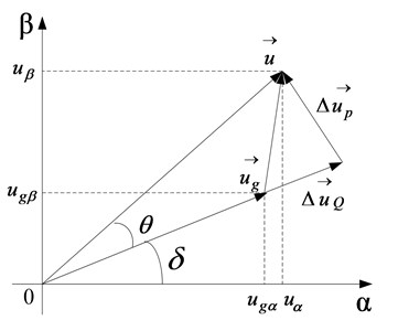
Fig. 6Phase diagram between grid-connected voltages and three-phase AC output voltages
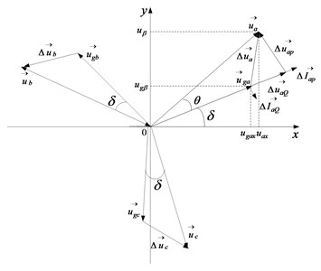
From Fig. 5, we have:
where:
According to Eq. (20) and Clark inverse transformation, the phase relationship between grid voltage space vector and AC output voltage space vector is shown in Fig. 6.
For A phase, in reference direction, then reactive current whose phase is lagging 90 degrees compared to grid voltage can be generated across inductor , active current whose phase is the same as grid is produced simultaneously by across inductor .Similarly for B and C phases.
Output power of each phase for inverter is:
where, is the fundamental angular frequency of the grid.
According to Eqs. (20) and (21), the target voltage space vector is calculated and input signal of SVPWM can be get naturally. Finally, the connection and break of devices in three-phase inverter arm are controlled by SVPWM to realize the decoupling between active power and reactive power.
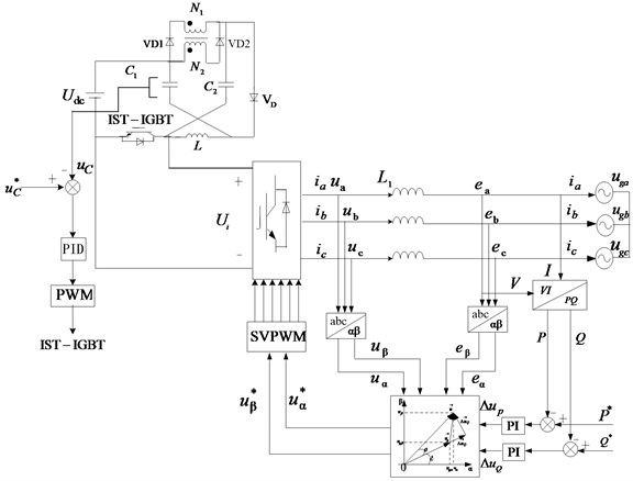
From above theoretical analysis, schematic diagram of IST-ZST-WCI grid-connected control can be shown as Fig. 7.
As can be seen, for the voltage loop, it is used to regulate dc-link voltage indirectly. The capacitor voltage is sampled, compared with its reference value and difference between them is sent to PID controller. Then IST-IGBT is driven by output signal of PID controller.
For the power loop, the actual output of the active power and reactive power are sampled and compared with their references and difference between them are sent to two PI controllers. Then, according to Eq. (21), output voltage references and can be calculated and regarded as the input signals for SVPWM to control the connection and break of devices in three-phase inverter bridge.
Fig. 7Control principle diagram of IST-ZSI-WCI
3.3. Double closed-loop controllers design
Double closed-loop controllers design is shown in Fig. 8. For Fig. 8(a), the actual capacitor voltage signal is collected and compared with its reference value, then difference between them are sent to regulator and regulated by it to ensure can track its reference value accurately and reach optimum effect. The same control process for power with power loop is get in block diagram Fig. 8(b).
Fig. 8System control block diagram

a) Capacitor voltage loop block diagram

b) Power loop control block diagram
3.4. Stability analysis with double closed-loop controller
According to linear control theory [20], the characteristic of can be defined as:
The poles of are the roots of the characteristic equation . In complex plane, if all poles are located on the left of the imaginary axis, the system characterized by can be seen stable, and instable if there is one pole located on the right side of the imaginary axis or imaginary axis in the complex plane, inversely.
The use of state feedback can change the transfer function of the system, is converted to GC(s), i.e. and then characteristic equation changes from to correspondingly, the roots of the characteristic equation are changed meanwhile. In other words, to get desired properties, we can apply various feedback matrix to change the location of zeros and poles. for they have significant influence on the characters of the system. In this paper, from Fig. 7 and Fig. 8, we can select suitable to change the location of the zeros and poles, so that the expected dynamical properties can be obtained.
4. Matlab-based simulation
Verification of the parameters chosen: the inductances of coupled inductor: 190 μH, 5 mH, turns ratio of ideal transformer: 4, Coupled coefficient 0.98, DC-side input voltage 120 V, the modulation ratio 0.8, shoot-through duty ratio 0.3, and the impedance network 100 μF, 6 mH. Modulation strategy of SVPWM in which the trigger pulse is applied alone to make IST-IGBT conduct is used in this paper. Verification results are as follows:
Input DC voltage is shown in Fig. 9(a), the DC voltage across the inverter is shown in Fig. 9(b).
Fig. 9Features of novel Z-Source inverter
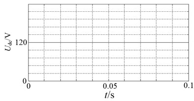
a) Input DC voltage
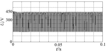
b) Dc-link voltage across the inverter
As can be seen from Fig. 9, when DC input voltage is 120 V, dc-link voltage is 430 V accordingly. Showing that this inverter achieves a greater degree of boost.
The output waveforms of dc-link voltage and primary and secondary winding of coupled inductor current as well as the inductor current in passive network are shown in Fig. 10.
It can be seen from Fig. 10 that waveforms are in line with above theoretical analyses and verifying the correctness of theoretical analysis.
As shown in Fig. 11, by controlling of capacitor loop, capacitor voltage of the Z-source inverter always follows its reference value.
Fig. 12 shows that when 0.05 s, the DC power voltage descends from 120 V to 90 V, dc-link voltage of the Z-source inverter is hardly affected by the fluctuation of DC power voltage, quickly restored to its original value after a minor fluctuation. Proving that under the control of the voltage loop, this system has good robustness and is suitable for power fluctuation occasions.
When the active and reactive power reference value are stated respectively as 8.5 kW, 0 VAR, the tracking waveforms of the actual output active power and reactive power are given in Fig. 13. As can be seen from figures, under the control of power loops, the actual output power values track their reference values. Indicating that the active and reactive powers can be controlled independently, i.e. decoupled excellently by this control strategy.
Fig. 10The waveform of structure and principle for the novel Z-Source inverter
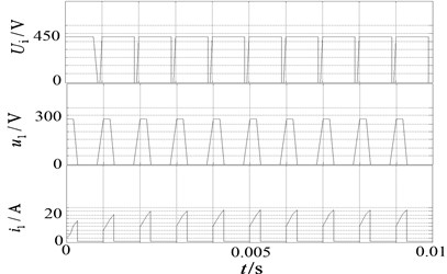
a) is DC voltage across the inverter, and are respectively the voltage of and current for the primary winding of coupled inductor
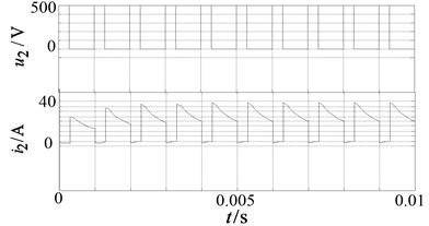
b) and are the voltage and current for secondary winding of the coupled inductor
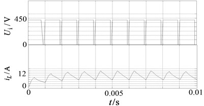
c) is dc-link voltage, is the inductor current in passive network
Fig. 11Waveform of DC-link voltage tracking reference voltage

Fig. 12DC-link waveform of input voltage changing
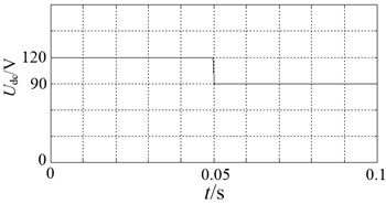
a) Input DC voltage
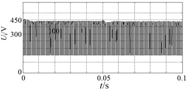
b) Dc-link voltage across the inverter
Fig. 13Waveform of power tracking

Fig. 14 shows the waveforms of three-phase grid voltages and currents. It can be visible that they are in phase and the novel Z-source system runs under the condition of higher power factor.
Fig. 14Current and voltage waveforms of grid-connected IST-ZSI-WCI

5. Conclusion
This paper proposes a novel Z-source inverter called improved Z-source inverter with coupled inductor which is introduced coupled inductor and its position relative to three-phase inverter is different from traditional Z-source inverter. Simulation validates that the novel Z-source inverter has much higher boost capacity and lower capacitor voltage stress during steady state, and then smaller size and weight of the devices can be used for this economical topology. Because of its position relative to the three-phase inverter being changed, inrush current will not exist at startup so that components in the circuit can avoid damage done by inrush current. Finally, shoot-through zero vectors are inserted solely through full-controlled device IST-IGBT in SVPWM modulation strategy to make the separation between boost factor and modulation factor and thus improve the boost capacity as well as quality of AC voltage .Aiming at the novel Z-source inverter, it was modeled in frame ,avoid cross-coupling of current state variables and then, dual loops control strategy with PI controller including a voltage loop and a power loop are introduced to control the inverter connecting to the grid. Simulation results showed that under the condition of the control strategy, the novel system achieve unity power factor running and has good dynamic property and robustness. Verifying that the novel Z-source inverter has many superior performances and broad application prospects.
References
-
Fang Zheng Peng Source inverter. IEEE Transactions on Industry Applications, Vol. 39, Issue 2, 2003.
-
Praveen K. P., Ravishankar A. N. Simulation of a hybrid energy system using multiple input DC-DC converter and Z-source inverter with maximum boost control strategy. International Conference on Computation of Power, Energy, Information and Communication, 2014, p. 250-255.
-
Gu J. Y., Chen G. C. A fast MPPT algorithm for single-stage grid-connected PV inverter. ACTA Energiae Sinica, Vol. 35, Issue 1, 2014, p. 154-160.
-
Li X. L., Zhou Y. S., Li S. P. The Improvement of control technology for voltage source PWM inverter. Electrical Measurement and Instrumentation, Vol. 50, Issue 574, 2013, p. 119-123.
-
Yi L. Z., Peng H. M., Wang G. P., He S. F., Zou X., Li M., Chen Y. R. Study of decoupling control algorithm based on grid line voltage space vector in three-phase photovoltaic grid-connected inverter. ACTA Energiae Sinica, Vol. 31, Issue 1, 2010, p. 72-78.
-
Peng F. Z., Shen M., Holland K. Application of Z-source inverter for traction drive of fuel cell-battery hybrid electric vehicle. IEEE Transactions on Power Electronics, Vol. 22, Issue 3, 2007, p. 1054-1061.
-
Cui B., Qian Z. M., Ding X. P., Peng F. Z. A voltage-current close loop control algorithm for Z-source inverter. Power Electronics, Vol. 41, Issue 9, 2007, p. 1-3.
-
Cai C. W., Qu B. Y., Kuang K. Enhanced Z-source inverters. Proceedings of the CSEE, Vol. 31, 2011, p. 259-266.
-
Yang S. T., Ding X. P., Zhang F., Qian Z. M. Study on Z-source inverter for photovoltaic generation system. Proceedings of the CSEE, Vol. 28, Issue 17, 2008, p. 112-118.
-
Zhang L. J., Tan G. J., Chen L. P. Neutral point potential balance control for three-level Z-source Inverters based on double modulation wave technique. Power System Protection and Control, Vol. 41, Issue 7, 2013, p. 91-96.
-
Li Y., Peng F. Z. Constant capacitor voltage control strategy for Z-source/quasi Z-source inverter in grid-connected photovoltaic systems. Transactions of China Electrotechnical Society, Vol. 26, Issue 5, 2011, p. 62-69.
-
Tang Yu, Xie Shaojun, Zhang Chaohua Improved Z-source inverter. Proceedings of the CSEE, Vol. 29, Issue 30, 2009, p. 28-34.
-
Zhou Y. F., Huang W. X., Zhao J. W. Tapped inductor quasi Z-source inverters. Proceedings of the CSEE, Vol. 32, Issue 27, 2012, p. 126-133.
-
Liu X., Loh P. C., Wang P., Han X. Improved modulation schemes for indirect Z-source matrix converter with sinusoidal input and output waveforms. IEEE Transactions on Power Electronics, Vol. 27, Issue 9, 2012, p. 4039-4050.
-
Zhu M., Yu K., Luo F. L. Switched-inductor Z-source inverter. IEEE Transactions on Power Electronics, Vol. 25, Issue 8, 2010, p. 2150-2158.
-
Vinnickov D., Roasto I. Quasi-Z-source-based isolated DC/DC converters for distributed power generation. IEEE Transactions on Industrial Electronics, Vol. 58, Issue 1, 2011, p. 192-201.
-
Loh P. C., Vilathgamuwa D. M., Lai Y. S., Chua G. T., Li Y. W. Pulse width modulation of Z-source inverters. IEEE Transactions on Power Electronics, Vol. 20, 2005, p. 1346-1355.
-
Banaei M. R., Dehghanzadeh A. R., Salary E. Z-source inverter based multilevel inverter with reduction of switches. IET Power Electronics, Vol. 5, Issue 3, 2012, p. 385-392.
-
Meenakshi T., Rajambal K. Identification of an effective control scheme for Z-source inverter. Asian Power Electronic Journal, Vol. 4, Issue 1, 2010, p. 22-28.
-
Zheng D. Linear Control Theory. Ting hua University Press, Beijing, 2003.
About this article
This work is supported by the National Natural Science Foundation of China (Grant No. 61263004) and Gansu Province Natural Science Foundation (Grant No. 1212RJZA071).
