Abstract
The proposed research suggests an improvised performance which is efficient and a reliable converter as a reasonable solar photo Voltaic (PV) approach. The proposed research helps in elevating the performance levels so that power extraction is maximized from the respective PV arrays specifically during the case of limited shading. In order to track the maximum amount of power from every solar PV string, connection of DC-DC converters is done amid the solar PV strings. By doing so, maximum power output can be ensured by the operation of each string irrespective of the occurrence of variation in the solar radiation amongst diverse strings. Usually, the DC-DC converter that would be employed for this purpose would process the string’s power completely. This Full Power Processing (FPP) architecture gives rise to extreme losses of conversion. Hence, the suggested work propound a Partial Power Processing (PPP) that processed a part of the total system power, while the rest of the power is straight away delivered to the output side, thus provides high conversion efficiency when compared to the existing DC-DC FPP converters. An input parallel output series structure having a novel Non-Isolated Partial Power Processing topology (NIPPP) is recommended and the operation’s details are elucidated depending on the operating principle. For the purpose of evaluating the performance of the converter, Matlab Simulink environmental platform are carried out. The closed loop prototype experimental approach is also carried out with the improvement of efficiency compared to conventional it appears in efficient manner.
Highlights
- CVC converter has a continuous input and output current characteristics because of two inductors, the output current ripples are approximately zero, which makes it to have a low power loss.
- The output voltage can be increased or decreased so that the converter is high reliable.
- The proposed PPP architecture, the chief portion of the Photovoltaic power is reliably fed to the load thus it is necessary for the converter to process a significantly minimal amount of power.
- To design enhanced Buck converter involving lesser components for reducing the current conduction losses.
- To regulate the load voltage highly in all the power flow situations by employing three-domain load voltage control method.
1. Introduction
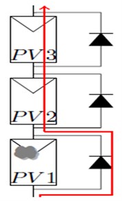
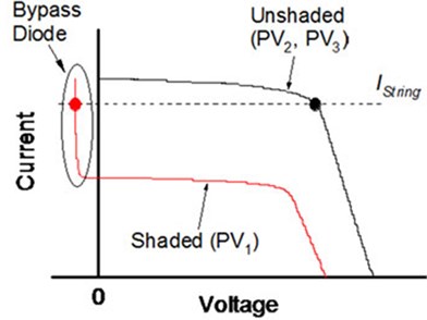
By means of incessant cost reduction as well as technological progress development, the photovoltaic (PV) mounted globally has caused an inclination towards exponential growth in the generation capacity. Nevertheless, one of the major tests in the utilization of a PV source is resolving its inherent low-voltage compatibility by using an electrical load. PV modules present as a series connection can provide a practical solution to the issue of voltage matching but experiencing partial shading on a PV substrings leads to drastic reduction in the utilization of energy. Usually, the substring currents are reliant on irradiance; furthermore the shaded substrings are not that proficient in current generation when compared to un-shaded ones. Supposing the shaded substrings are not anymore capable of generation of a string current, the parallel connected bypass diodes begin the conduction in order to circumvent the shaded substrings, as denoted in Fig. 1(a), resulting in a considerable mismatch in the operational voltage [1]. The I-V features of the shaded as well as un-shaded modules prevalent at similar temperatures except at different levels of insulation are depicted in Fig. 1(b). It is the Central converter which has the ability to extract the overall characteristic’s peak pertaining to the PV array that might be considered to be lower than the summation of the existing maximum power of every module in the array because of the mismatch losses that occur at the time of shading [2].
Fig. 1PV string under partial shading condition: a) Bypassed substring, b) I-V characteristics string characteristics
a)
b)
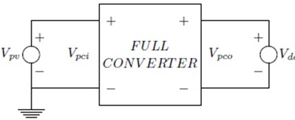
In order to remove the effects of mismatches as well as to augment the power output, at the substring level, the power might be processed by the application of Full Power Processing (FPP) architectures and Partial Power Processing (PPP) architectures denoted in Fig. 2(a) and Fig. 2(b), 2(c) respectively as Input Parallel Output Series (IPOS) and Output Parallel Input Series(ISOP). In the FPP architecture, processing of the entire PV string’s output power is performed by the converter. In comparison to the boost and buck-boost converter, the buck converter is considered to be the most efficient [3] possessing a low operating range. For the purpose of enhancing the efficiency as well as the operation over a wide range of PV voltage, a bridge based topology of buck/boost is proposed in [4, 5]. This can function in modes like buck, boost as well as pass through. With the absence of any disparity in the string, the FPP converter still requires complete processing of the PV power. This leads to an increased loss in power.
Considering a PPP architecture, the chief portion of the PV power is reliably fed to the load thus it is necessary for the converter to process a significantly minimal amount of power. The amount of power processed by the converter is considered to be equal to the product of the PV string current as well as a small voltage introduced in the series to the PV string. This gives rise to decreased power rating of the converter. Additionally, it might give rise to reduced conversion losses in comparison to FPP. Furthermore, while there is no mismatch amidst the strings, no power is processed by PPP, thus elevating the overall efficiency. For the purpose of analyzing the processed power by the converter, a variable referred to as partial power ratio Kpr is established as:
where Ppco and Ppv denote the power processed by the converter and the power distributed by the PV module, respectively. Subsequently, the converter functioning as a PPP relates to a partial power ratio less than unity Kpr < 1.
The following research paper has been arranged as follows. Section 2 introduces a comparative study of PPP architectures possessing few key candidate topologies. Section 3 elucidates the proposed PPP scheme operation, analytical equations as well as its control. In the Section 4 simulation case study of the suggested converter at partial shading PV condition employing a cascaded topology is explained. Section 5 presents the calculation of losses. Section 6 shows the performance analysis of the proposed converter as well as the simulation result of the suggested converter along with the dynamic irradiance variation. Section 7 encloses the concluding remarks.
Fig. 2Full power converter and two possible partial power converters
a) Full power processing
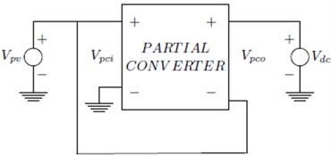
b) Partial power process I in the IPOS structure
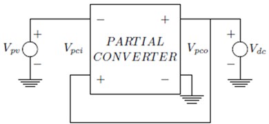
c) Partial power process II in the ISOP structure
2. Materials and methods
Due to various converter topologies, the SEPIC has a pulsating output current this will lacks the output voltages and not regulated. Similarly, Ćuk converter does not have negative output polarity, unless the isolated Ćuk converter is used but for no-isolated it’s also not regulated the output voltage required to the load. To overcome this situation basic DC-DC converter is proposed with improved manner for PV power.
Partial Power Processing (PPP) usually is categorized as a dual kind of approach on account of its inherent presence as well another significant aspect of it being as a violation of the respective isolation transformer two approaches are:
• Isolated partial power processing (IPPP).
• Non-isolated partial power processing (NIPPP).
With respect to IPPP that has been categorized as the two series module full bridge Converter [6], LLC Resonant converter [7] as well as the full bridge with partial power processing which may be deployed to fulfill the purpose of constructing high-power-density converters. As these function, almost seamlessly at high switching frequencies and as having a natural zero-voltage switching, there is an inherent disadvantage of them lacking on account of low partial load efficiency. The respective converter mode of operation continues as being complex and costly affair on account of two main integral factors which are basically the topology design and implantation and extent of control. Structure and detailing of Fig. 2(b) and Fig. 2(c) [8-10] has been shown in the same manner with the Input Parallel Output Series (IPOS) flyback converter as well as the Input Series Output Parallel (ISOP) flyback converter. This has been proven to specifically useful in the case of simple modes as it also delivers extremely high efficiency. The same is also deployed in the case of low-power-density applications that are executed with a specific limited voltage transformation ratio as well as the deployment of the regulation ability application.
Considering NIPPP where this high-power application functions are deployed in easy and efficient operation modes. Also, there is no requirement for the high-frequency transformer as this helps in process of simplifying the design and also minimizing associated costs and time. Though there is an inherent disadvantage that limits its performance on account of the inherent features of the power structures. There are two possible results if the requirement of isolation is violated. The first result is a potential short circuit if a boost converter is used to realize the partial power process I in the IPOS structure shown in Fig. 2(b), the source will be shorted directly to ground [10]. Similar result in the loss of the merits of handling partial power if a flipped buck converter or a regular buck-boost converter is used to realize the partial power process II in the ISOP structure shown in Fig. 2(c), they are equivalent to a full power processing (FPP) [10-20].
Wu Deng proposed [21], an improved ant colony optimization (ICMPACO) algorithm based on the multi-population strategy, co-evolution mechanism, pheromone updating strategy, and pheromone diffusion mechanism is proposed to balance the convergence speed and solution diversity and improve the optimization performance in solving the large-scale optimization problem. In the proposed ICMPACO algorithm, the optimization problem is divided into several sub-problems and the ants in the population are divided into elite ants and common ants in order to improve the convergence rate and avoid to fall into the local optimum value. The pheromone updating strategy is used to improve optimization ability.
Motor bearing is subjected to the joint effects of much more loads, transmissions, and shocks that cause bearing fault and machinery breakdown. A vibration signal analysis method is the most popular technique that is used to monitor and diagnose the fault of motor bearing. However, the application of the vibration signal analysis method for motor bearing is very limited in engineering practice. In this paper, on the basis of comparing fault feature extraction by using empirical wavelet transform (EWT) and Hilbert transform with the theoretical calculation, a new motor bearing fault diagnosis method based on integrating EWT, fuzzy entropy, and support vector machine (SVM) called EWTFSFD is proposed by Wu Deng [22].
Wu Deng [23] The dynamic fractional calculus with memory characteristic is used to reflect the trajectory information of particle updating in order to improve the convergence speed. The Alpha-stable distribution theory is used to replace the uniform distribution in order to escape from the local minima in a certain probability and improve the global search ability. Next, the DOADAPO algorithm is used to solve the constructed multi-objective optimization model of gate assignment in order to fast and effectively assign the gates to different flights in different time. Finally, the actual flight data in one domestic airport is used to verify the effectiveness of the proposed method.
Wu Deng [24], the proposed MGACACO algorithm makes use of the exploration capability of GA and stochastic capability of ACO algorithm. In the proposed MGACACO algorithm, the multi-population strategy is used to realize the information exchange and cooperation among the various populations. The chaotic optimization method is used to overcome long search time, avoid falling into the local extremum and improve the search accuracy. The adaptive control parameters is used to make relatively uniform pheromone distribution, effectively solve the contradiction between expanding search and finding optimal solution.
Wu Deng [25] The fuzzy information entropy values of IMFs are calculated to reveal the intrinsic characteristics of the vibration signal and considered as feature vectors. Then the diversity mutation strategy, neighborhood mutation strategy, learning factor strategy and inertia weight strategy for basic particle swarm optimization (PSO) algorithm are used to propose an improved PSO algorithm. The improved PSO algorithm is used to optimize the parameters of least squares support vector machines (LS-SVM) in order to construct an optimal LS-SVM classifier, which is used to classify the fault. Finally, the proposed fault diagnosis method is fully evaluated by experiments and comparative studies for motor bearing.
Wu Deng [26] proposed A damage degree identification method based on high-order difference mathematical morphology gradient spectrum entropy (HMGSEDI) is proposed in this paper to solve the problem that fault signal of rolling bearings are weak and difficult to be quantitatively measured. In the HMGSEDI method, on the basis of mathematical morphology gradient spectrum and spectrum entropy, the changing scale influence of structure elements to damage degree identification is thoroughly analyzed to determine its optimal scale range. The high-order difference mathematical morphology gradient spectrum entropy is then defined in order to quantitatively describe the fault damage degree of bearing.
The existing all type of IPPP which is discussed in this paper above are output Kinetic Energy, so we have proposed a system for NIPPP of Current-Voltage-Current energy transport mechanism where the output is Kinetic Energy. The NIPPP based Current-Voltage-Current (CVC) Converter is proposed with modified IPOS structure shown in Fig. 3(a) and its equivalent circuit diagram shown in Fig. 3(b). The converter part basic resistive load are carried for analysis and to find the efficiency of the converter.
Fig. 3Proposed partial power CVC converters
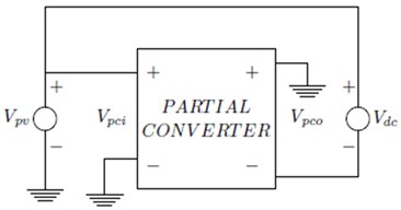
a) Modified partial power converter I in the IPOS structure
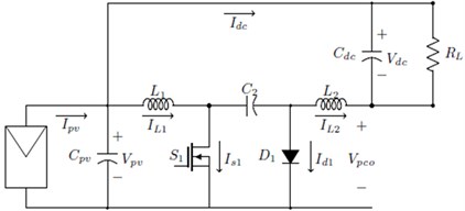
b) Partial power CVC converter
2.1. Circuit topology
In this section, we design CVC partial power converters for a voltage step-up application and compare it to a full power converter. First, we focused on the step-up voltage application, the output voltage is the sum of the PV string voltage and the voltage of converter. Since this converter does not need to process all the input power, the overall conversion efficiency is very high. The converter has a very simple topology composed of only one switching device (S1), one diode (D1), two Capacitors (C1, Cdc) and two Inductors (L1, L2). The switches and diodes have to withstand the total output voltage. The CVC converter is operated in both step up and step down mode. The output voltage can be increased or decreased so that the converter is high reliable. In contrast, CVC converter has a continuous input and output current characteristics, and because of two inductors, the output current ripples are approximately zero, which makes it to have a low power loss.
The CVC converter operates in two operating modes in the MPPT design. The first mode of operation is shown in Fig. 4(a), when the switch (S1) is closed (ON), and the diode (D1) is in the reverse-biased state. In this mode, because of Vc1 > Vdc, the capacitor C1 and PV supplies power energy for output DC bus capacitor and inductor (L2) at the same while the pv discharge its a huge part partial power energy for L1 inductor. The theoretical continuous conduction mode (CCM) waveforms during switch on time (0 to t0) is shown in Fig. 5.
Fig. 5DC equivalent circuit of CVC converter
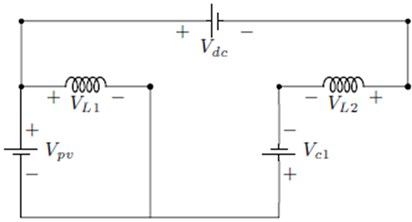
a) Mode 0
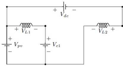
b) Mode 1
The equations for the switch on conduction mode are as follows:
The second mode of operation is shown in Fig. 4(b), when the switch (S1) is open (OFF) and the diode (D1) is in the forward-biased state. In this mode, C1 is charged by Vpv and VL1 through the diode (D1), and the output DC bus capacitor (Cdc) harvests energy from inductor L2 and PV supply through the diode (D1). The theoretical CCM waveforms during switch off time (t0 to t1) is shown in Fig. 6.
Fig. 6Theoretical CCM waveforms during one switching period Ts for the CVC converter
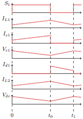
The equations for the switch off conduction mode are as follows:
The converter operates in ON state from t= 0 to t=D∙T (D is the duty cycle), and in OFF state from D∙T to T (that is, during a period equal to ((1-D)∙T). The average values of VL1 and VL2 are therefore:
The principles of CVC converter operating conditions state that the average values of the periodic inductor voltage and capacitor current waveforms are zero when the converter operates in steady state:
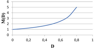
The CVC converter conversion ratio M is given in the following equation, the CVC converter conversion ratio M versus the duty cycle variation is shown in Fig. 7, where M:
The inductor and capacitor value of the converter is calculated by considering 10 % voltage ripple and current ripple. The following equations are used to design the CVC converter:
where fsw is the switching frequency of the MOSFET switch.
Fig. 7CVC converter conversion ratio M
2.2. Control of DC-DC converter
The control scheme is shown in Fig. 8, for partial power CVC converters. In order to extract the maximum power, a Perturb and Observe (P&O) MPPT algorithm [14] is performed because of the simple implementation and effective tracking [15, 16]. A cascaded control loop is implemented where the given voltage reference V*pv, from the MPPT algorithm, is controlled by an external PI controller, and the current reference I*L1, is controlled by an internal PI controller. The output signal represents the duty cycle D, which gives the required signal to drive the converter.
Fig. 8DC-DC control scheme

2.2.1. Simulation of proposed converter at partial shading.
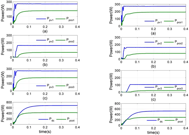
In order to valid the effectiveness of the topology in mitigating the mismatch in series connected strings; three strings with proposed CVC converter using cascaded topology are simulated in MATLAB/Simulink environment. The simulated system is shown in Fig. 9 and system Specifications are listed in Table 1. Two cases are considered:
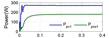
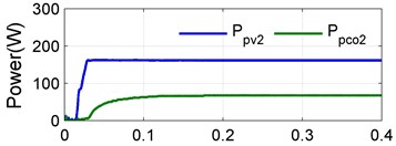
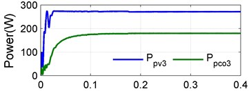
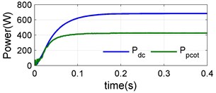
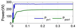
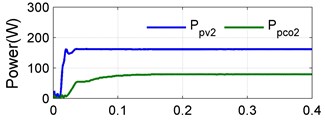
Case 1 (single shaded PV): In this case one PV is considered to be shaded. The irradiations levels of the first, second and third strings are assumed to be 1000 W/m2, 600 W/m2 and 1000 W/m2, The simulated produces a PV power Ppv1= 273 W, Ppv2= 161 W and Ppv3= 273 W, process a converter power Ppco1= 179 W, Ppco2= 67.4 W and Ppco3= 179 W. The power of shaded second PV string is transfer to dc bus to obtain maximum the dc power Pdc= 683 W is shown in Fig. 10.
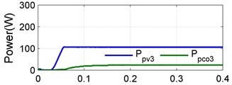
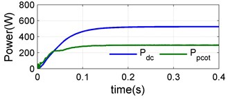
Case 2 (dual shaded PV): In this case two PV’s are shaded. The irradiations levels of the first and second are as in case 1, third strings is assumed 300 W/m2. This simulation system produced a PV power Ppv3= 106 W process a converter power Ppco3= 23 W the power of shaded second and third pv strings is transfer to dc bus to obtain maximum the dc power Pdc= 524 W is shown in Fig. 11.
Table 1Simulation parameter
Variable | Parameter | Value |
Ppv | PV power | 275 W |
Vmpp | Voltage at Max power | 31 V |
Impp | Current at Max power | 8.87 A |
VOC | PV open circuit voltage | 36 V |
ISC | PV short circuit current | 9.21 A |
NCELL | Number of cells | 60 |
L1 | Input Inductor | 1 mH |
L2 | Output Inductor | 2 mH |
C1 | Capacitor | 100 uF |
Cdc | DC capacitor | 400 uf |
fsw | Switching frequency | 25 Khz |
Fig. 9CVC converter cascaded topology
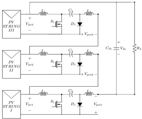
Fig. 10Case 1: a) PV power and converter power for string 1, b) PV power and converter power for string 2, c) PV power and converter power for string 3, d) DC power and total converter power
a)
b)
c)
d)
Fig. 11Case 2: a) PV power and converter power for string 1, b) PV power and converter power for string 2, c) PV power and converter power for string 3, d) DC power and total converter power
a)
b)
c)
d)
2.2.2. Calculation
In this section losses are estimated based on the above selection, semiconductor devices and other components, also to evaluate reliability PV voltage, converter voltage and dc voltage is obtain for same operating level.
2.3. Losses calculation
(i) MOSFET conduction loss: In the on-state MOSFET exhibit a finite resistance at the time of device conducts this result in conduction power loss. Based on the waveform for current through switches, rms current is calculated. The RMS value of the switch current of CVC converter is shown in Fig. 11(b). Conduction loss is obtained by square of the rms current multiplied by the Rds:
where Rds. is the drain-source on-state resistance, I2S1rms switching rms current.
(ii) MOSFET switching loss: For estimation of switching loss, switching trajectory is considered linear. Switching loss (turn-on and turn-off losses) of MOSFET are given by:
where uds1 represent the power switch off-state zero-current drain-source voltages, the switching frequency is fs, and tc(on) and tc(off) are the power switch turn-on and turn-off transition times, respectively. It should also be noted that uds1 is the power switch drain-source voltage when the switch is off as shown in Fig. 11(a).
(iii) Diode conduction loss: Diode conduction loss is calculated from the expression:
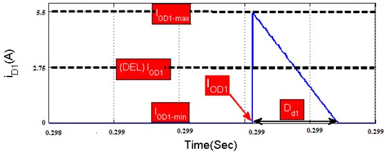
RMS (ID1rms) and Average (ID1) value of diode current is calculated Based on the waveform of diode current shown in Fig. 11(d).
(iv) Winding Copper loss: Due to the finite resistance of Inductor L1 and L2 winding, power is dissipated in the form of heat. The expression of L1 and L2 winding losses of CVC converter are given by:
(V) Diode losses. For the diode losses (D1) the loss due to forward voltage is determined in Eq. (18) and its circuit are shown in Fig. 12:
Fig. 12Diode loss of proposed converter
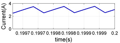
The temperature effect on the copper loss is neglected. Where IL1rms and IL2rms inductor RMS current is calculated from the waveform show in Fig. 13(c) and Fig. 13(e), respectively.
Fig. 13Switching waveform of: a) switch S1 voltage (Vs1), b) switch S1 current (Is1), c) inductor L1 current (IL1), d) diode D1 current (Id1), e) Inductor L2 current (IL2)

a)

b)

c)

d)
e)
To reduce the stress on its devices, the Continuous Conduction Mode (CCM) is preferred as an operating mode of the CVC converter. Fig. 13 presents the converter indices such as Vs1, Is1,IL1, Id1 and IL2. These switching waveform manifest a CCM operation of the CVC converter and a limited device stress.
2.4. Dynamic variation and performance comparison
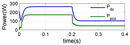
In order to validate the proposed converter and control scheme the dynamic performances, a step in the irradiation is obtain at simulated time t= 0.2 s, from 1000 W/m2 to 400 W/m2 to demonstrate the systems satisfactory dynamic behavior in Fig. 14. The 1000 W/m2 irradiation produced a PV power of 273.6W delivers 268 W power to load at the efficiency of 98.14 %, processed by the converter power of 181 W with the partial power ratio,Kpr= 64.3 %, and at 400 W/m2 irradiation produced a PV power of 105.5 W delivers 104.2 W power to load at the efficiency of 98.79 %, processed by the converter power of 48 W with the partial power ratio Kpr= 44.29 % is calculated. For various PV power, the simulation values of partial power ratio and efficiency of 98.6 % are calculated using the measured converter power and switching on proposed converter, which are presented in Fig. 14(a) and Fig. 14(b).
Fig. 14(a). represents the waveforms of Vpv, Vpco and Vdc. A changeover of the proposed converter form the boost mode to buck mode takes place according to a variation in the climatic condition. An advancement in the irradiance from 1000 W/m2 to 400 W/m2 leads to an decrease in Vpco 58.4 V to 25.3 V, Vpv 31.35 V to 30.25 V and Vdc from 89.75 V to 55.55 V, its clearly shows that Vpv<Vpco in 1000 W/m2 andVpv>Vpco in 400 W/m2 is operated in boost mode and buck mode respectively. Fig. 14(c) shows the proposed converter buck/boost operating range at different irradiation.
Fig. 14Transient step response results for the proposed CVC converter

a)

b)

c)

d)
e)
2.5. Experimental setup
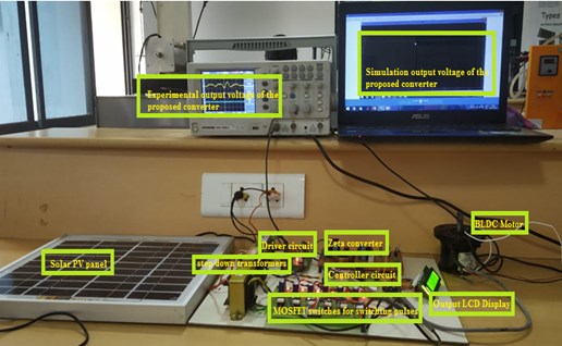
The experimental setup of the proposed system is consists of control circuit, driver circuit, converter circuit as shown in Fig. 16. The projected power flow management system is experimented by implementing the state house model. The values of the passive parts used are a 100 H for boost electrical device L, a 1000Hz frequency for input electrical condenser Cin and output capacitor Co. A fifty W star PV module with Associate in MPP voltage of 24 V DC and MPP current of 2.44 A and electric battery with 24 V DC are used as power sources. The reference voltage of the standalone BLDC motor is ready at 48 V DC.
Fig. 15Simulation results under different input power/irradiation
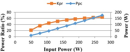
a) Partial power ratio and power handled by the converter
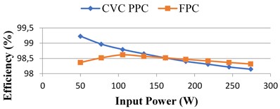
b) Converter efficiency
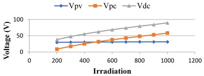
c) CVC converter buck/boost operating range
Fig. 16Experimental prototype of proposed converter
2.6. Experimental results
The switch S1 determines the converter switching pulse and it is shown in Fig. 17.
The switching pulse S2 determines the converter gate voltage of 2.4 volts is shown Fig. 18.
Fig. 17Switching pulse S1

The magnitude and time period of the input voltage of the transformer to the converter are shown in Fig. 19.
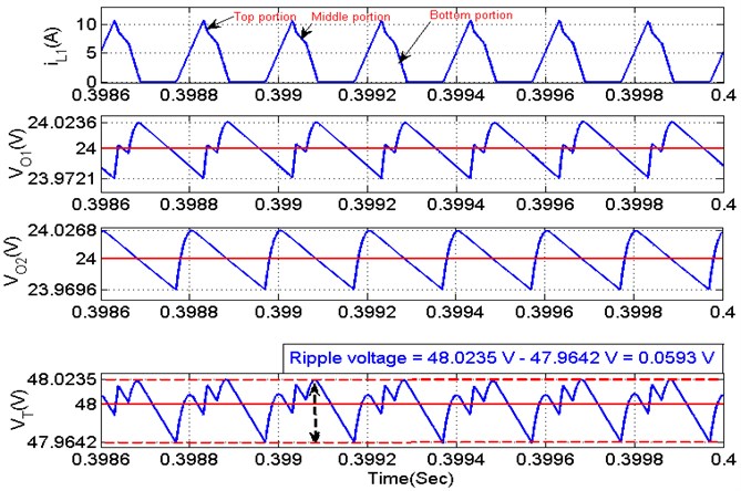
The boost circuit increases the voltage from 16 V to 48 V and also reduces the losses in the circuit as shown in Fig. 20 and its ripple voltage are also shown in Fig. 21.
Fig. 18Switching pulse S2

Fig. 19Input voltage to the converter

Fig. 20Output voltage of the boost converter

Fig. 21Ripple voltage performance of proposed converter
The Comparison of various conventional converter are carried out with the proposed converter as a result the proposed is occurred as efficient are its chart are shown in Fig. 22. The Table 2 shows the various comparison of converter with the proposed. The proposed converter peak settling time and peak overshoot period are also calculated and determined as shown in Table 3.
Fig. 22Comparison chart of proposed converter with conventional converter
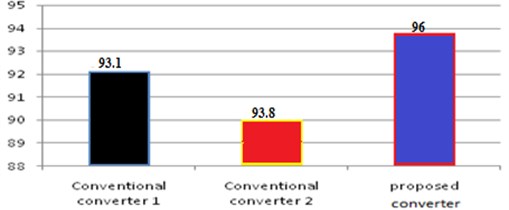
Table 2Comparison of various converter with the proposed
S. No. | Objects | Conventional converter 1 | Conventional converter 2 | Proposed converter |
(Sathish Kumar et.al 2017) [20] | (Sathish Kumar et.al 2016) [27] | |||
1 | No of switches | 2 | 2 | 4 |
2 | Efficiency | 93.1 | 93.8 | 96 |
3 | Conduction losses | High | Medium | Low |
4 | Conversion topology | Boost | Buck-Boost | Buck-Boost |
5 | Switching frequency | 5 kHz | 5 kHz | 10 kHz |
6 | Turns ratio of transformer | 01:06 | 01:07 | 01:03 |
Table 3Peak settling time and peak overshoot period
At initial step input | Input voltage (V) | Load (%) | Output voltage (V) | Peak overshoot | Peak rise (ms) | Peak fall (ms) | Delay Time (ms) | PMSM drive | Frequency |
Input | 17 | 100 | 0-24 | 19 | 2.35 | 133 | 2.3 | Half value 15 W | 5 kHz |
24 | 100 | 48 | 6 | – | 90 | – | Full value 30 W | 5 kHz | |
Load | 17 | 100 | 0-24 | 11 | 2.35 | 133 | 2.3 | Half value 15 W | 5 kHz |
12 | 50 | 48 | 1.1 | 1.6 | 48 | – | Full value 20 W | 10 kHz |
3. Conclusions
The proposed research presents the design and performance analysis of a CVC Partial Power Processing (PPP) topology. Several aspects of the design and operation are improved in comparison to a Full Power Processing (FPP) scheme based on boost converter, such as a higher efficiency of the DC-DC conversion and a small power rating for the converter. Dynamic performance is analyzed by varying irradiance and is observed that the power handled by the proposed scheme is lesser when compared to the existing schemes. Also, the converter losses are reduced, and efficiency is improved. Simulation result of the variations in solar irradiation, the power handled by a partial power converter remains lower compared with a full power converter, it leads to smaller conversion losses and a greater efficiency, also Simulation result of CVC converter with three PV strings cascaded topology for different case of shading is included to verify the operation. The reduced ripple voltages and the efficiency of the converter achieved is 96 %, which is more efficient compared to conventional one.
References
-
Maki A., Valkealahti S. Power losses in long string and parallel connected short strings of series-connected silicon-based photovoltaic modules due to partial shading conditions. IEEE Transactions on Energy Conversion, Vol. 27, Issue 1, 2012, p. 173-183.
-
Patel Hiren, Agarwal Vivek MATLAB-based modeling to study the effects of partial shading on PV array characteristics. IEEE Transactions Energy Convers, Vol. 23, Issue 1, 2008, p. 302-310.
-
Walker G. R., Sernia P. C. Cascaded DC converter connection of photovoltaic modules. IEEE Transactions Power Electronics, Vol. 19, Issue 4, 2004, p. 1130-1139.
-
Walker G. R., Pierce J. Photo voltaic DC-DC module integrated converter for novel cascade and bypass grid connection topologies-design and optimization. 37th IEEE Power Electronics Specialists Conference, 2006.
-
Kaushika N., Gautam N. Energy yield simulations of interconnected PV arrays. IEEE Transactions on Energy Conversion, Vol. 18, Issue 1, 2003, p. 127-134.
-
Lee J., Min B., Kim T., Yoo D., Yoo J. High efficient interleaved input-series-output-parallel-connected converter for photovoltaic power conditioning system. IEEE Energy Conversion Congress and Exposition, 2009.
-
Chen Liqun, Wu Hongfei, Xu Peng A high step-down non-isolated bus converter with partial power conversion based on synchronous LLC resonant converter. IEEE Applied Power Electronics Conference and Exposition, 2015.
-
Ahmad Md Waseem, Anand Sandeep Power decoupling in PV system using partial power processing converter. 10th International Conference on Compatibility, Power Electronics and Power Engineering, 2016.
-
Zapata Jaime W., Renaudineau Hugues, et al. Partial power DC-DC converter for photovoltaic microinverters. 42nd Annual Conference of the IEEE Industrial Electronics Society, 2016.
-
Zhao Junjian, Yeates Kenton, Han Yehui Analysis of high efficiency converter processing partial input/output power. IEEE 14th Workshop on Control and Modeling for Power Electronics, 2013.
-
Agamy Mohammed S. An efficient partial power processing converter for distributed PV architectures. IEEE Transactions on Power Electronics, Vol. 29, Issue 2, 2014, p. 674-686.
-
Agamy M. S., Chi S., Elasser A., Harfman Todorovic M., Jiang Y., Mueller F., Tao F. A high power density DC-DC converter for distributed PV architectures. IEEE Journal of Photovoltaics, Vol. 3, Issue 2, 2013, p. 791-798.
-
Teuvo Suntio Comments on an efficient partial power processing converter for distributed PV architectures. IEEE Transactions on Power Electronics, Vol. 30, Issue 4, 2015, p. 2372.
-
Kouro S., Wu B., Abu Rub H., Blaabjerg F. Photovoltaic Energy Conversion systems. Power Electronics for Renewable Energy Systems, Transportation, and Industrial Applications, 1st Edition, Wiley, 2014.
-
Elgendy Mohammed A., Bashar Zahawi Assessment of perturb and observe MPPT algorithm implementation techniques for PV pumping applications. IEEE Transactions on Sustainable Energy, Vol. 3, Issue 1, 2012, p. 21-33.
-
Dezso Sera, Laszlo Mathe, Tamas Kerekes, Sergiu Viorel Spataru, Remus Teodorescu On the perturb-and-observe and incremental conductance MPPT methods for PV systems. IEEE Journal of Photovoltaics, Vol. 3, Issue 3, 2013, p. 1070-1078.
-
Zientarski Jonatan Rafael Rakoski, Pinheiro José Renes, Martins Mário Lúcio Da Silva, Hey Hélio Leães Understanding the partial power processing concept: a case-study of buck-boost DC-DC series regulator. IEEE 13th Brazilian Power Electronics Conference and 1st Southern Power Electronics Conference, 2015.
-
Kasper Matthias, Bortis Dominik, Kolar Johann W. Classification and comparative evaluation of PV panel-integrated DC-DC converter concept. IEEE Transactions on Power Electronics, Vol. 29, Issue 5, 2014, p. 2511-2526.
-
Min Byung-Duk, Lee Jong-Pil, Kim Jong-Hyun, Kim Tae-Jin, Yoo Dong-Wook, Song Eui-Ho A new topology with high efficiency throughout all load range for photovoltaic PCS. IEEE Transactions on Industrial Electronics, Vol. 56, Issue 11, 2009, p. 4427-4435.
-
Sathish Kumar Meenakumari S. R. Design and implementation of six switch three phase inverter BLDC motor drive for commercial applications. Asian Journal of Research in Social Sciences and Humanities, Vol. 6, Issue 7, 2016, p. 1301-1310.
-
Deng Wu, Xu Junjie, Zhao Huimin An improved ant colony optimization algorithm based on hybrid strategies for scheduling problem. IEEE Access, Vol. 7, 2019, p. 20281-20292.
-
Deng Wu, Zhang Shengjie, Zhao Huimin, Yang Xinhua A novel fault diagnosis method based on integrating empirical wavelet transform and fuzzy entropy for motor bearing. IEEE Access, Vol. 6, 2018, p. 35042-35056.
-
Deng Wu, Zhao Huimin, Zou Li, Li Guangyu, Yang Xinhua, Wu Daqing A novel collaborative optimization algorithm in solving complex optimization problems. Applied Soft Computing, Vol. 59, 2017, p. 288-302.
-
Deng Wu, Zhao Huimin, Zou Li, Li Guangyu A novel collaborative optimization algorithm in solving complex optimization problems. Soft Computing, Vol. 21, Issue 15, 2017, p. 4387-4398.
-
Deng Wu, Zhao Huimin, Zou Li, Li Guangyu, Yang Xinhua, Wu Daqing A novel intelligent diagnosis method using optimal LS-SVM with improved PSO algorithm. Soft Computing, Vol. 23, Issue 7, 2019, p. 2445-2462.
-
Deng Wu, Zhao Huimin, Zou Li, Li Guangyu, Yang Xinhua, Wu Daqing Study on a novel fault damage degree identification method using high-order differential mathematical morphology gradient spectrum entropy. Entropy, Vol. 20, 2018, p. 682.
-
Sathish Kumar Shanmugam, Mahendran Krishnamoorthy, Krishnakumar Kanagaraj, Meenakumari Ramachandran Solar power based DC-DC converter fed brushless DC motor drive for agricultural applications. Indian Journal of Ecology, Vol. 45, Issue 1, 2018, p. 25-32.

