Abstract
Continuous developments in the field of 3D printing techniques and equipment have enabled their usage in the field of electronics structures, circuits, and device fabrication in addition to many other fields. This advancement has enabled the potential fabrication of sensors using silicon-based micro or even Nanoelectronics. Currently, the manufacturing and packaging of such devices and structures are heavily reliant on lithography, which can be slow and can involve substantial processing requirements. In this paper, a temperature-sensing Interdigital Transducer (IDT) structure was designed and fabricated using Direct Laser Writing (DLW) based on Two-Photon Lithography (TPL), which is a high-resolution 3D printing technology. The TPL in a positive photoresist was combined with the physical vapor deposition method and the lift-off process to create gold IDT microstructures. The developed sensing structures were characterized using a network analyzer to determine the resonance frequency and its dependence on the temperature changes. The results showed that the IDT structures exhibit a linear response toward the changes in temperature with an average sensitivity of 0.123 MHz/°C. The most important advantage in producing the IDT structure with the additive manufacturing technique is that a very small-sized structure is produced error-free and efficiently.
1. Introduction
The application-based technological developments with customer requirements accelerated the development of sensor technology in many fields. Sensors are the main mechatronic system components that detect changes in the environment through mechanical or non-mechanical stimulations such as pressure, stiffness, roughness, and temperature [1-2]. The preferred manufacturing technology, selected materials, and the required response time are the most important factors in sensor technology. These factors are important in sensor fabrication.
Developments in industrial applications have started to require more micro and nano-scale devices. This need requires sensor systems to be produced in smaller sizes for a wide variety of industrial applications [3-5]. Micro and Nano Electro-Mechanical Systems (MEMS/NEMS) are used in transportation sectors such as automotive [6] and aviation [7], energy [8], robotics [9-10], optics [11], biomedical [12] and geophysics [13]. MEMS devices function as biosensors in medical research and contribute to many promising studies [14]. These sensors can reduce very wet laboratories to a microchips [15]. In addition to the solutions produced for the electrical [16-17], and construction [18] sectors, they also have applicability in knowledge and labor-intensive fields such as mechanics and chemistry. Although these devices are a single unit, they also have electrical and mechanical components. These devices can measure changes in physical quantities such as temperature, pressure, viscosity, stress, and mass [19-25]. Devices called laboratories on chips have become increasingly preferred in biomedical and bioengineering fields [26]. These devices with reduced geometric dimensions can react much faster and will continue to be more attractive as more efficient and portable devices [27-28]. Of course, in addition to these superior features, there are also some limitations. The most important of these is the need for simultaneous perception and execution in an environment while associating it with mutually exclusive mechanisms [29-30]. To overcome these limitations, single-platform devices capable of detecting acoustic waves have been proposed for simultaneous sensing and actuation. Such devices are known as Surface acoustic waves (SAW) sensors. These devices are widely used not only as sensors and actuators but also as filters, oscillators, and transformers. The applications here are made possible by the use of piezoelectric components as the central backbone of SAW sensors [31-34].
As is known, SAW-based sensors can be fabricated using a cleanroom facility and conventional [35] or next-generation mask lithography. These complex several-step processes [36] are difficult to follow; Graphenic sensitive layers can be used in the manufacturing of new generation surface acoustic wave (SAW) sensors developed with a graphene sensitive layer. When this type of sensor is produced, low cost, easy manufacturability and superior performances can be achieved. In fact, within the capabilities of production technology, producing nano-sized products can increase the advantages mentioned. Studies on graphenic precision layer SAW sensors are ongoing. [37]. It is also known that there are individual layers that come together spontaneously. Therefore, with the rapid development of microprocessors and the development of software tools, SAW designs with complex structures in terms of both geometry and materials can be proposed. This revealed the need for new manufacturing technologies that could be used quickly to produce the proposed new designs. In this context, direct writing techniques have emerged as a promising approach in sensor fabrication. Au et al. [38] compared the cost of a sensor produced traditionally, that is, through lithography, with that of 3D printing technology. In stereolithography, the difference was found to be 15 USD [39]. The fact that the 3D printing technique is both low-cost and simple to produce has made it very attractive to reproduce the same structure with minimum human effort. Additionally, the sensitivity and accuracy of the printed sensor are affected compared to traditional methods [40-41]. Among the direct writing methods, Ink-jet printing provides improved flexibility in terms of both design customization and substrate size [42]. However, the need for miniaturized devices limits the use of this method as the line resolution is in the order of a few tens of micrometers. To improve spatial resolution, direct laser writing methods (DLW) are particularly interesting as they allow the fabrication on demand of customized complex structures with submicron resolution [43, 44].
DLW using a UV beam was introduced to create micro-supercapacitor devices onto a graphite oxide film. Other DLW-based techniques were reported in the literature. They allow the fabrication of sensors by laser fusion of silver laser reduction of graphene oxide, and laser micromachining. However, these techniques are limited to some specific materials [45].
In that context, Two-Photon Lithography (TPL) in positive photoresists combined with material deposition and lift-off is an interesting alternative approach as it allows the rapid fabrication of complex designs in a large choice of materials. In addition, TPL allows an increase in spatial resolution due to the non-linear absorption process and some photochemical effects [46-49]. Fabrication using TPL [50, 51] evolved in the 90s [52] and has found its application in many different fields including but not limited to biosensing [53-55], micro and nano-optics [56-61], robotics [62, 64], security [65].
This work focuses on the use of TPL combined with physical vapor deposition of Gold for the fabrication of an Interdigital Transducer (IDT) based passive temperature sensor. As compared to the conventional lithography techniques, Two-Photon Lithography (TPL) stands out from traditional fabrication methods by eliminating the need for physical masks in the creation of IDTs for acoustic wave sensors. This mask-free approach offers greater flexibility, precision, and customization options, making TPL particularly advantageous for rapidly prototyping and tailoring IDT designs to specific sensor applications [66-69]. Moreover, combined with physical or chemical vapor deposition methods and lift-off, TPL in positive photoresists offers the advantage of fabricating IDT structures with a large number of materials (metals and metal oxides) [70-73].
2. Materials and methods
2.1. Material determination for sensor fabrication
Material selection is very important in sensor design. Because the performance, sensitivity, accuracy, and reliability of the sensors are highly dependent on the materials used in their construction. The thermal, mechanical, electrical, and chemical properties of the materials to be selected are directly affected by the sensitivity of the sensor to be produced, its signal-noise properties, and its environmental compatibility [74, 75]. Gold as a material for IDTs is important in certain high-frequency applications with its high electrical conductivity, chemical stability, ease of processing, and low insertion loss in certain frequency ranges. It has low acoustic attenuation, meaning it can maintain the intensity of sound waves passing through it with minimal loss [76, 78] This feature is useful in applications where sound transmission efficiency is paramount. It has a relatively high refractive index for sound waves. Also, since gold is not a good acoustic damper, it does not dampen sound waves [79-81]. For these reasons, the IDT structure in our study was made from gold.
2.2. Sensor design
The dimensions of the proposed single port IDT structure, presented in Figure 1, are provided in Table 1.
Fig. 1Design and design parameters of the proposed IDT sensing structure. COMSOL was used during the designing phase
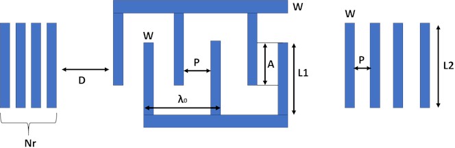
Table 1Summary of geometric parameters for the proposed IDT structures
Parameter | Size in µm |
Thickness of the design | 2 |
Electrode finger width (W) | 3 |
Distance between electrodes (P) | 6 |
IDT length (reflectors) (L2) | 80 |
IDT length (L1) | 100 |
Distance between IDT and reflectors (D) | 3 |
Distance between two IDTs (λ0) | 21 |
Aperture (A) | 92.5 |
Number of reflectors (Nr) | 15 |
Number of IDT pairs (Ni) | 30 |
Fig. 1 describes the structural design parameters for the proposed resonator-based temperature sensor. As depicted in Fig. 1, the IDT structure is designed with a certain pitch among them and the resulting surface acoustic wave is well-founded when the pitch of the IDT fingers and the wavelength of the surface wave are equal to each other. Eq. (1) is employed to determine the resonant frequency (f), which is a function used for measuring the temperature, of the proposed structure and its relation to the propagation velocity (Vr) of the resulting surface wave:
where λ is the wavelength of the SAW. The IDT structure needs to be quantified to develop its model. Fig. 1 and Table 1 show the labeled IDT structure and its explanation respectively. To achieve the strongest IDT activation and phase superposition of SAW, the IDT pitch, which is W+P, should be equal to half of the SAW wavelength, as described by the wave interference principle. Therefore:
The distance (D) between the IDT and the adjacent reflectors should also satisfy equation 3 to make sure that IDT receives the standing wave on its peak:
The aperture width of the IDT fingers also plays an important role in the performance of the SAW resonator. Normally, it is between 50 and 100 times the SAW wavelength.
2.3. Fabrication
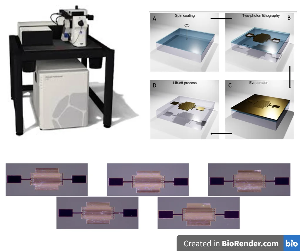
Nanoscribe GmbH’s Photonic Professional GT was utilized for the fabrication of the sensing structure. The fabrication setup was based on a DLW system using TPL in a positive photoresist. This system implemented a femtosecond fiber laser source which was operating at 780 nm wavelength. The power of the deployed laser source was between 50-150 mW with 80 MHz of repetition rate. The laser source produced a pulse length of 100-200 femtoseconds.
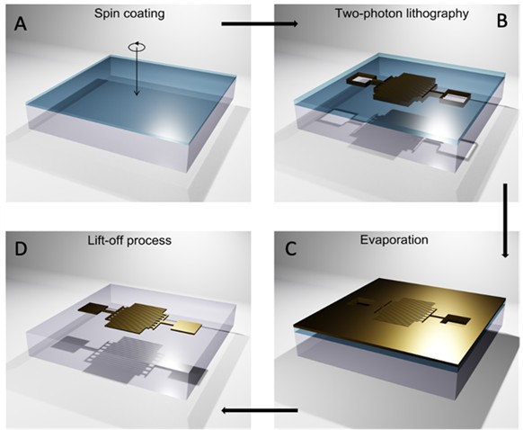
The fabrication process of IDT structures made from gold on a glass substrate is shown in Fig. 2. The dimension of the glass substrate used for this fabrication process was size 22 mm×22 mm with a thickness of 170 µm. The substrate was cleaned before the realization of the printing process. Later on, 60 % v/v of MICROPOSIT S1813 positive photoresist was deployed on the surface of the substrate. The sample was then spin-coated onto the substrate at 4000 RPM for 30 seconds using a Karl Suss CT62 spin-coating machine (Fig. 2(a)). After the completion of the spin coating process, a layer of approximately 500 nm in thickness was achieved. The sample was then exposed using Nanoscribe GmbH’s Photonic Professional GT (Fig. 2(b)). The magnification and the numerical aperture of the objective were 63x and 1.4 respectively. After the TPL sept, the sample was developed using the MF-319 developer solution for 30 seconds at room temperature. Then the sample was cleaned by immersing it in deionized water. After development, 5 nm of chromium and 30 nm of gold were successively deposited on the sample by physical vapor deposition (Fig. 2(c)). The chromium was used to improve the adhesion of gold on the glass substrate. To remove the remaining photoresist from the sample, a lift-off process was employed by immersing the prepared sample in acetone and keeping it there for 10 hours (Fig. 2(d)). Finally, the sample was rinsed using de-ionized water and blow-dried using air.
Fig. 2Fabrication workflow for the printing of IDT structures using TPL followed by physical vapor deposition of gold and lift-off. (Renderings are done through the software Blender)
2.4. IDT structures characterizations
– Electron scanning microscopy; by using a sputter coater SC7640 from Quorum Technologies, the samples were metalized. A Field Emission Gun (FEG Hitachi SU8030) operating at 10 kV was used to perform scanning electron microscopy (SEM).
– Optical microscopy; A Nikon Eclipse LV100 upright microscope was used to capture optical microscopy images.
– Resonance frequency measurements.
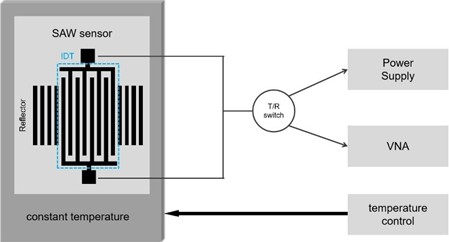
The fabricated IDT structures were tested using a network analyzer to measure their frequency response and to determine the resonance frequency. The general representation of the setup is shown in Fig. 3.
Fig. 3Schematic diagram of the setup for temperature response
3. Results. Printed IDT
Following the workflow shown in Fig. 2 several IDT structures, shown in Fig. 4, were fabricated using the DLW technique. Scanning Electron Microscopy (SEM) images of one of the fabricated IDT structures are shown in Fig. 5.
Fig. 4The Fabricated IDT structures using DLW technique
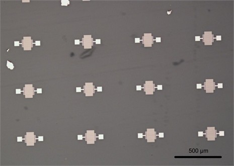
Fig. 5SEM images of the fabricated IDT structure
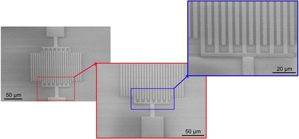
Fig. 6Frequency response of the fabricated IDT structures
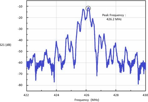
The frequency response of the developed sensor is shown in Fig. 6. The resonance frequency of the designed structure was predicted to be 424.01 MHz by the theoretical calculations and simulations. From the experiments, the value of resonance frequency was measured as 426.2 MHz. Comparing these two results, the deviation of 0.5 % is well within the acceptable range.
The illustration of the test setup is shown in Fig. 3. The optical microscope image of the IDTs used for temperature response analysis is given in Fig. 7. The frequency response of the fabricated IDTs was measured from 20 °C to 100 °C with a step size of 5 °C. The results are presented in Fig. 8.
Fig. 7Optical microscope image of the IDTs used for temperature response analysis
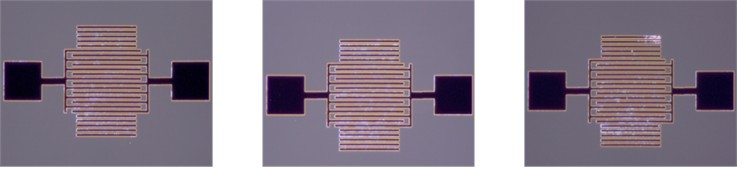
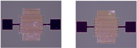
Fig. 8Temperature response of the five analyzed IDT structures. Each IDT structure was analyzed 10 times. Each point in the figures a)-e) corresponds to the average frequency measured for a given temperature, f) is the average of the responses of the 5 IDT structures. The red line is a linear fit
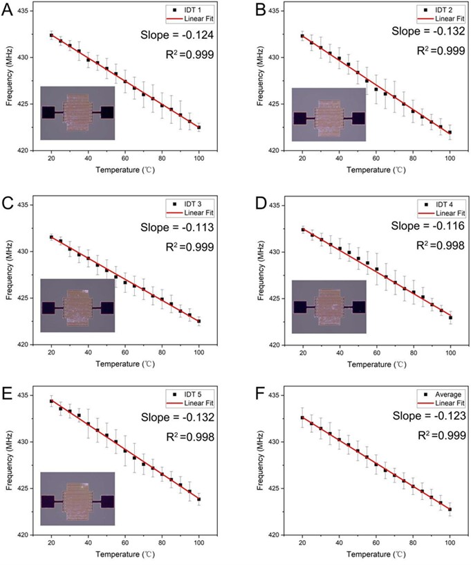
The fabricated IDT structures show very good linearity when tested against temperature. The average sensitivity is 0.123 MHz/°C. The average R2 values from 10 tests for each IDT structure along with the combined average value are shown in Fig. 8. The results show that the IDT structures exhibit a linear response towards the temperature changes.
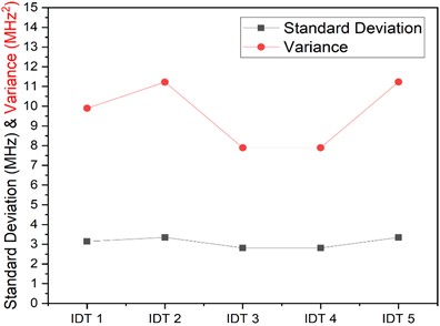
The standard deviation and variance plot for each IDT is presented in Fig. 9. This variation can be due to more than one reason. Even though the conditions during the testing were mostly the same, it is possible that external noise and interference were present. Factors such as electromagnetic interference or acoustic noise can introduce additional variability in the observed response.
Fig. 9Standard deviation and variance plot for the fabricated IDTs
4. Conclusions
In this study, the micro-sized heat sensor is produced using the layered manufacturing technique. The 2PP method was used as a mask in the layered production technique. Usable results were obtained in the tests and analyzes of the heat sensor produced with this technique. The most important advantage in producing the IDT structure with the additive manufacturing technique is that a very small-sized structure is produced error-free and efficiently
The electron microscope images of the fabricated IDT structures showed consistency of the employed printing method with the proposed design. The frequency response of the fabricated IDT structures was measured using a test setup and the peak frequency was found to be 426.2 MHz. The simulations gave only a slightly deviating resonant frequency of 424.01 MHz. The results of those tests showed their response to be very much linear with the temperature changes. The average R2 value of all the responses was > 0.99.
References
-
L. Zou, C. Ge, Z. Wang, E. Cretu, and X. Li, “Novel tactile sensor technology and smart tactile sensing systems: a review,” Sensors, Vol. 17, No. 11, p. 2653, Nov. 2017, https://doi.org/10.3390/s17112653
-
M. I. Tiwana, S. J. Redmond, and N. H. Lovell, “A review of tactile sensing technologies with applications in biomedical engineering,” Sensors and Actuators A: Physical, Vol. 179, No. 17, pp. 17–31, Jun. 2012, https://doi.org/10.1016/j.sna.2012.02.051
-
A. S. Algamili et al., “A review of actuation and sensing mechanisms in MEMS-based sensor devices,” Nanoscale Research Letters, Vol. 16, No. 1, p. 16, Jan. 2021, https://doi.org/10.1186/s11671-021-03481-7
-
S. Ersoy and T. Waqar, “Surface acoustic wave sensing,” in Encyclopedia of Sensors and Biosensors, Elsevier, 2023, pp. 129–141, https://doi.org/10.1016/b978-0-12-822548-6.00103-5
-
B. Shih et al., “Design considerations for 3D printed, soft, multimaterial resistive sensors for soft robotics,” Frontiers in Robotics and AI, Vol. 6, p. 30, Apr. 2019, https://doi.org/10.3389/frobt.2019.00030
-
Bhatt et al., “Sensors for automotive and aerospace applications,” in Energy, Environment, and Sustainability, Vol. 12, Singapore: Springer Singapore, 2019, pp. 223–239, https://doi.org/10.1007/978-981-13-3290-6
-
H. D. Ngo, “A novel piezoresistive microphone MEMS sensor for aerospace applications,” in International Conference on Electrical, Computer and Energy Technologies, pp. 1–5, 2022.
-
H. Li et al., “3D printed flexible triboelectric nanogenerator with viscoelastic inks for mechanical energy harvesting,” Nano Energy, Vol. 58, pp. 447–454, Apr. 2019, https://doi.org/10.1016/j.nanoen.2019.01.066
-
I. S. Bayer, “MEMS-based tactile sensors: materials, processes and applications in robotics,” Micromachines, Vol. 13, No. 12, p. 2051, Nov. 2022, https://doi.org/10.3390/mi13122051
-
T. An, S. Yoon, and J. Kim, “Additive manufacturing of inductive force sensor with NiZn-ferrite magnetic core for robotic gripper,” Additive Manufacturing, Vol. 71, p. 103600, Jun. 2023, https://doi.org/10.1016/j.addma.2023.103600
-
X. Chen, H. Wang, and X. Wei, “A wide bandwidth real-time MEMS optical power meter with high resolution and linearity,” Sensors and Actuators A: Physical, Vol. 339, p. 113506, Jun. 2022, https://doi.org/10.1016/j.sna.2022.113506
-
C. Chircov and A. M. Grumezescu, “Microelectromechanical systems (MEMS) for biomedical applications,” Micromachines, Vol. 13, No. 2, p. 164, Jan. 2022, https://doi.org/10.3390/mi13020164
-
H.-F. Liu et al., “A review of high-performance MEMS sensors for resource exploration and geophysical applications,” Petroleum Science, Vol. 19, No. 6, pp. 2631–2648, Dec. 2022, https://doi.org/10.1016/j.petsci.2022.06.005
-
M. Mehdipoor and H. Badri Ghavifekr, “Design and analysis of a new MEMS biosensor based on coupled mechanical resonators for microfluidics applications,” Analog Integrated Circuits and Signal Processing, Vol. 111, No. 2, pp. 277–286, Feb. 2022, https://doi.org/10.1007/s10470-021-01963-3
-
J. Zhu et al., “Development trends and perspectives of future sensors and MEMS/NEMS,” Micromachines, Vol. 11, No. 1, Dec. 2019, https://doi.org/10.3390/mi11010007
-
M. Xu et al., “Design and fabrication of an absolute pressure MEMS capacitance vacuum sensor based on silicon bonding technology,” Vacuum, Vol. 186, p. 110065, Apr. 2021, https://doi.org/10.1016/j.vacuum.2021.110065
-
S. Ersoy, G. Atakok, D. Khorsandi, and E. Toptaş, “Investigation of time-based pressure control for microfluidics chip design,” Journal of Engineering Research, May 2022, https://doi.org/10.36909/jer.14067
-
Q. Meng and S. Zhu, “Developing IoT sensing system for construction-induced vibration monitoring and impact assessment,” Sensors, Vol. 20, No. 21, p. 6120, Oct. 2020, https://doi.org/10.3390/s20216120
-
S. P. Parida and P. C. Jena, “Dynamic analysis of cracked FGM cantilever beam,” in Lecture Notes in Mechanical Engineering, Vol. 1, Singapore: Springer Singapore, 2020, pp. 339–347, https://doi.org/10.1007/978-981-15-2696-1_33
-
P. Singh, K. Sharma, I. Puchades, and P. B. Agarwal, “A comprehensive review on MEMS-based viscometers,” Sensors and Actuators A: Physical, Vol. 338, p. 113456, May 2022, https://doi.org/10.1016/j.sna.2022.113456
-
S. Scott, High Pressure Rheology for Quantitative Electrohydrodynamic. Elsevier, 2019.
-
P. Ripka and A. Tipek, Modern Sensors Handbook. London, UK: Wiley, 2010, https://doi.org/10.1002/9780470612231
-
K. S. Raju, Fluid Mechanics, Heat Transfer, and Mass Transfer: Chemical Engineering Practice. John Wiley & Sons, 2011.
-
A. Bhattad, “Review on viscosity measurement: devices, methods and models,” Journal of Thermal Analysis and Calorimetry, Vol. 148, No. 14, pp. 6527–6543, 2023, https://doi.org/10.1007/s10973-023-12214
-
S. P. Parida, S. Sahoo, and P. C. Jena, “Prediction of multiple transverse cracks in a composite beam using hybrid RNN-mPSO technique,” Proceedings of the Institution of Mechanical Engineers, Part C: Journal of Mechanical Engineering Science, Mar. 2024, https://doi.org/10.1177/09544062241239415
-
S. P. Parida, P. C. Jena, S. R. Das, D. Dhupal, and R. R. Dash, “Comparative stress analysis of different suitable biomaterials for artificial hip joint and femur bone using finite element simulation,” Advances in Materials and Processing Technologies, Vol. 8, No. sup3, pp. 1741–1756, Oct. 2022, https://doi.org/10.1080/2374068x.2021.1949541
-
D. Mark, S. Haeberle, G. Roth, F. Von Stetten, and R. Zengerle, “Microfluidic lab-on-a-chip platforms: requirements, characteristics and applications,” Chemical Society Reviews, Vol. 39, No. 3, p. 1153, Jan. 2010, https://doi.org/10.1039/b820557b
-
T. A. Franke and A. Wixforth, “Microfluidics for miniaturized laboratories on a chip,” ChemPhysChem, Vol. 9, No. 15, pp. 2140–2156, Oct. 2008, https://doi.org/10.1002/cphc.200800349
-
M. A. Kartal, G. Atakök, and S. Ersoy, “Cooling and multiphase analysis of heated environmentally friendly R152A (C2H4F2) fluid coming from the production process according to Nist indicators,” Applied Sciences, Vol. 14, No. 10, p. 4143, May 2024, https://doi.org/10.3390/app14104143
-
Y. Dağdelen, F. Akyüz, A. Feyzioğlu, and E. Toptaş, “Design and analysis of a 4-axis cartesian robot for unloading plastic injection machines in industrial applications,” Journal of Mechatronics and Artificial Intelligence in Engineering, Vol. 4, No. 2, pp. 104–111, Dec. 2023, https://doi.org/10.21595/jmai.2023.23553
-
T. Waqar and S. Ersoy, “Design and analysis comparison of surface acoustic wave-based sensors for fabrication using additive manufacturing,” Journal of Nanomaterials, Vol. 2021, pp. 1–12, Jun. 2021, https://doi.org/10.1155/2021/5598347
-
I. Unalli, S. Ersoy, and I. Ertugrul, “Microfluidics chip design analysis and control,” Journal of Mechatronics and Artificial Intelligence in Engineering, Vol. 1, No. 1, pp. 2–7, Jun. 2020, https://doi.org/10.21595/jmai.2020.21470
-
H. Sun, S. Huang, and L. Peng, “High-current sensing technology for transparent power grids: a review,” IEEE Open Journal of the Industrial Electronics Society, Vol. 5, pp. 326–358, Jan. 2024, https://doi.org/10.1109/ojies.2024.3387432
-
S. Qureshi, M. Hanif, V. Jeoti, G. M. Stojanović, and M. T. Khan, “Review of fabrication of SAW sensors on flexible substrates: Challenges and future,” Results in Engineering, Vol. 22, p. 102323, Jun. 2024, https://doi.org/10.1016/j.rineng.2024.102323
-
S. Cao, N. Weerasekera, and D. R. Shingdan, “Modeling approaches for fluidic mass transport in next generation micro and nano biomedical sensors,” European Journal of Biomedical Research, Vol. 1, No. 3, pp. 1–9, May 2022, https://doi.org/10.24018/ejbiomed.2022.1.3.12
-
M. Araya-Farias, S. Dziomba, and N. T. Tran, “Microfluidic strategies for extraction and preconcentration of proteins and peptides,” in Handbook on Miniaturization in Analytical Chemistry, Elsevier, 2020, pp. 35–75, https://doi.org/10.1016/b978-0-12-819763-9.00003-9
-
B. S. Damasceno et al., “Recent improvements on surface acoustic wave sensors based on graphenic nanomaterials,” Materials Science in Semiconductor Processing, Vol. 167, p. 107811, Nov. 2023, https://doi.org/10.1016/j.mssp.2023.107811
-
A. K. Au, W. Huynh, L. F. Horowitz, and A. Folch, “3D‐printed microfluidics,” Angewandte Chemie International Edition, Vol. 55, No. 12, pp. 3862–3881, Mar. 2016, https://doi.org/10.1002/anie.201504382
-
I. Kashkoush, J. Rieker, G. Chen, and D. Nemeth, “Process control challenges of wet etching large MEMS Si cavities,” in Solid State Phenomena, Vol. 219, Switzerland: Trans Tech Publications, Ltd., 2014, pp. 73–77, https://doi.org/10.4028/www.scientific.net/ssp.219.73
-
A. Bigham et al., “Advances in tannic acid-incorporated biomaterials: Infection treatment, regenerative medicine, cancer therapy, and biosensing,” Chemical Engineering Journal, Vol. 432, p. 134146, Mar. 2022, https://doi.org/10.1016/j.cej.2021.134146
-
D. Khorsandi et al., “Manufacturing of microfluidic sensors utilizing 3D printing technologies: a production system,” Journal of Nanomaterials, Vol. 2021, pp. 1–16, Aug. 2021, https://doi.org/10.1155/2021/5537074
-
E. N. Zare, P. Makvandi, and S. Ersoy, “Micro and nano sensors from additive manufacturing,” Journal of Nanomaterials, Vol. 2022, No. 1, Apr. 2022, https://doi.org/10.1155/2022/9835910
-
H. Luo, Y. Zhang, J. Yu, X. Dong, and T. Zhou, “Additive, subtractive and formative manufacturing of glass-based functional micro/nanostructures: A comprehensive review,” Materials and Design, Vol. 233, p. 112285, Sep. 2023, https://doi.org/10.1016/j.matdes.2023.112285
-
P. Mainik, C. A. Spiegel, and E. Blasco, “Recent advances in multi‐photon 3D laser printing: active materials and applications,” Advanced Materials, Vol. 36, No. 11, Dec. 2023, https://doi.org/10.1002/adma.202310100
-
G. Zyla and M. Farsari, “Frontiers of laser‐based 3D printing: a perspective on multi‐photon lithography,” Laser and Photonics Reviews, Vol. 18, No. 7, Mar. 2024, https://doi.org/10.1002/lpor.202301312
-
M. G. Mohammed and R. Kramer, “All‐printed flexible and stretchable electronics,” Advanced Materials, Vol. 29, No. 19, Mar. 2017, https://doi.org/10.1002/adma.201604965
-
A. K. Au, W. Lee, and A. Folch, “Mail-order microfluidics: evaluation of stereolithography for the production of microfluidic devices,” Lab Chip, Vol. 14, No. 7, pp. 1294–1301, Jan. 2014, https://doi.org/10.1039/c3lc51360b
-
Z. Zhan, J. An, Y. Wei, T. Tran, and H. Du, “Inkjet-printed optoelectronics,” Nanoscale, Vol. 9, No. 3, pp. 965–993, Jan. 2017, https://doi.org/10.1039/c6nr08220c
-
Y. Khan, A. Thielens, S. Muin, J. Ting, C. Baumbauer, and A. C. Arias, “A new frontier of printed electronics: flexible hybrid electronics,” Advanced Materials, Vol. 32, No. 15, Nov. 2019, https://doi.org/10.1002/adma.201905279
-
S. Khan, L. Lorenzelli, and R. S. Dahiya, “Technologies for printing sensors and electronics over large flexible substrates: a review,” IEEE Sensors Journal, Vol. 15, No. 6, pp. 3164–3185, Jun. 2015, https://doi.org/10.1109/jsen.2014.2375203
-
M. Berggren, D. Nilsson, and N. D. Robinson, “Organic materials for printed electronics,” Nature Materials, Vol. 6, No. 1, pp. 3–5, Jan. 2007, https://doi.org/10.1038/nmat1817
-
J. Perelaer et al., “Printed electronics: the challenges involved in printing devices, interconnects, and contacts based on inorganic materials,” Journal of Materials Chemistry, Vol. 20, No. 39, p. 8446, Jan. 2010, https://doi.org/10.1039/c0jm00264j
-
R. F. Pease and S. Y. Chou, “Lithography and other patterning techniques for future electronics,” Proceedings of the IEEE, Vol. 96, No. 2, pp. 248–270, Feb. 2008, https://doi.org/10.1109/jproc.2007.911853
-
A. Nathan et al., “Flexible electronics: the next ubiquitous platform,” Proceedings of the IEEE, Vol. 100, No. Special Centennial Issue, pp. 1486–1517, May 2012, https://doi.org/10.1109/jproc.2012.2190168
-
R. R. Søndergaard, M. Hösel, and F. C. Krebs, “Roll‐to‐roll fabrication of large area functional organic materials,” Journal of Polymer Science Part B: Polymer Physics, Vol. 51, No. 1, pp. 16–34, Oct. 2012, https://doi.org/10.1002/polb.23192
-
S. Moscato et al., “Additive manufacturing of 3D substrate integrated waveguide components,” Electronics Letters, Vol. 51, No. 18, pp. 1426–1428, Sep. 2015, https://doi.org/10.1049/el.2015.2298
-
D. L. Hine Tong, A. A. Manga, P. Minard, A. Delattre, L. Crowther-Alwyn, and P. Borel, “Comparative study of WLAN dual-band monopole antennas printed and etched on paper and PET substrates,” in 46th European Microwave Conference (EuMC), pp. 1243–1246, Oct. 2016, https://doi.org/10.1109/eumc.2016.7824575
-
Y. Morimoto, M. Memarian, X. Li, and T. Itoh, “Open-end microstrip line terminations using lossy gray-scale inkjet printing,” IEEE Transactions on Microwave Theory and Techniques, Vol. 65, No. 12, pp. 4861–4870, Dec. 2017, https://doi.org/10.1109/tmtt.2017.2716352
-
A. Sahu et al., “Robust microwave characterization of inkjet-printed coplanar waveguides on flexible substrates,” IEEE Transactions on Instrumentation and Measurement, Vol. 66, No. 12, pp. 3271–3279, Dec. 2017, https://doi.org/10.1109/tim.2017.2753384
-
J. J. Adams, S. C. Slimmer, J. A. Lewis, and J. T. Bernhard, “3D‐printed spherical dipole antenna integrated on small RF node,” Electronics Letters, Vol. 51, No. 9, pp. 661–662, Apr. 2015, https://doi.org/10.1049/el.2015.0256
-
J. Kimionis, M. Isakov, B. S. Koh, A. Georgiadis, and M. M. Tentzeris, “3D-printed origami packaging with inkjet-printed antennas for RF harvesting sensors,” IEEE Transactions on Microwave Theory and Techniques, Vol. 63, No. 12, pp. 4521–4532, Dec. 2015, https://doi.org/10.1109/tmtt.2015.2494580
-
T. Jungst, W. Smolan, K. Schacht, T. Scheibel, and J. Groll, “Strategies and molecular design criteria for 3D printable hydrogels,” Chemical Reviews, Vol. 116, No. 3, pp. 1496–1539, Feb. 2016, https://doi.org/10.1021/acs.chemrev.5b00303
-
B. Wendel, D. Rietzel, F. Kühnlein, R. Feulner, G. Hülder, and E. Schmachtenberg, “Additive processing of polymers,” Macromolecular Materials and Engineering, Vol. 293, No. 10, pp. 799–809, Oct. 2008, https://doi.org/10.1002/mame.200800121
-
S. El-Sayegh, L. Romdhane, and S. Manjikian, “A critical review of 3D printing in construction: benefits, challenges, and risks,” Archives of Civil and Mechanical Engineering, Vol. 20, No. 2, pp. 1–25, Mar. 2020, https://doi.org/10.1007/s43452-020-00038-w
-
Q. Yan et al., “A review of 3D printing technology for medical applications,” Engineering, Vol. 4, No. 5, pp. 729–742, Oct. 2018, https://doi.org/10.1016/j.eng.2018.07.021
-
Y. Zhang, X. Wang, K. Yan, H. Zhu, B. Wang, and B. Zou, “Laser micro/nano‐structuring pushes forward smart sensing: opportunities and challenges,” Advanced Functional Materials, Vol. 33, No. 8, Dec. 2022, https://doi.org/10.1002/adfm.202211272
-
D. S. Dkhar, R. Kumari, S. J. Malode, N. P. Shetti, and P. Chandra, “Integrated lab-on-a-chip devices: Fabrication methodologies, transduction system for sensing purposes,” Journal of Pharmaceutical and Biomedical Analysis, Vol. 223, p. 115120, Jan. 2023, https://doi.org/10.1016/j.jpba.2022.115120
-
H. Park et al., “Laser‐based selective material processing for next‐generation additive manufacturing,” in Advanced Materials, Wiley, 2023, https://doi.org/10.1002/adma.202307586
-
S. Mantihal, R. Kobun, and B.-B. Lee, “3D food printing of as the new way of preparing food: A review,” International Journal of Gastronomy and Food Science, Vol. 22, p. 100260, Dec. 2020, https://doi.org/10.1016/j.ijgfs.2020.100260
-
J. Fischer and M. Wegener, “Three‐dimensional optical laser lithography beyond the diffraction limit,” Laser and Photonics Reviews, Vol. 7, No. 1, pp. 22–44, Mar. 2012, https://doi.org/10.1002/lpor.201100046
-
S. Kawata, H.-B. Sun, T. Tanaka, and K. Takada, “Finer features for functional microdevices,” Nature, Vol. 412, No. 6848, pp. 697–698, Aug. 2001, https://doi.org/10.1038/35089130
-
H. Wang et al., “Two‐photon polymerization lithography for optics and photonics: fundamentals, materials, technologies, and applications,” Advanced Functional Materials, Vol. 33, No. 39, Mar. 2023, https://doi.org/10.1002/adfm.202214211
-
Z. Wang, H. Cui, A. Zhou, B. Li, and R. Gorgin, “Optimization design of an annular flexible IDT array based on a PDMS-PVDF substrate,” Journal of Intelligent Material Systems and Structures, Vol. 34, No. 18, pp. 2124–2132, Apr. 2023, https://doi.org/10.1177/1045389x231164532
-
A. Balena, M. Bianco, F. Pisanello, and M. de Vittorio, “Recent advances on high‐speed and holographic two‐photon direct laser writing,” Advanced Functional Materials, Vol. 33, No. 39, Feb. 2023, https://doi.org/10.1002/adfm.202211773
-
R. Kumar and N. Mandal, “SAW sensor basics on material, antenna, and applications: a review,” IEEE Sensors Journal, Vol. 24, No. 5, pp. 5713–5731, Mar. 2024, https://doi.org/10.1109/jsen.2024.3349656
-
J. Byeon, D. Kim, M. Kyeong, I. G. Bak, and S. Hong, “Acetal-functionalized indacenodithiophene (IDT): controlling the position of a Lewis acidic dopant for improved thermoelectricity,” Chemistry of Materials, Vol. 35, No. 5, pp. 2133–2145, Mar. 2023, https://doi.org/10.1021/acs.chemmater.2c03775
-
F. Lurz, T. Ostertag, B. Scheiner, R. Weigel, and A. Koelpin, “Reader architectures for wireless surface acoustic wave sensors,” Sensors, Vol. 18, No. 6, p. 1734, May 2018, https://doi.org/10.3390/s18061734
-
X. Li et al., “Advances in sensing mechanisms and micro/nanostructured sensing layers for surface acoustic wave-based gas sensors,” Journal of Materials Chemistry A, Vol. 11, No. 17, pp. 9216–9238, May 2023, https://doi.org/10.1039/d2ta10014b
-
S. S. Ba Hashwan et al., “A review of piezoelectric MEMS sensors and actuators for gas detection application,” Discover Nano, Vol. 18, No. 1, p. 25, Feb. 2023, https://doi.org/10.1186/s11671-023-03779-8
-
M. Agostini and M. Cecchini, “Ultra-high-frequency (UHF) surface-acoustic-wave (SAW) microfluidics and biosensors,” Nanotechnology, Vol. 32, No. 31, p. 312001, Jul. 2021, https://doi.org/10.1088/1361-6528/abfaba
-
Kadi et al., “Development of high frequency interdigital transducers for NDT of thin films,” in Forum Acusticum, 2020.
-
C. Wright and G. V. Hartland, “Mode specific dynamics for the acoustic vibrations of a gold nanoplate,” Photoacoustics, Vol. 30, p. 100476, Apr. 2023, https://doi.org/10.1016/j.pacs.2023.100476
About this article

This work has been made within the framework of the Graduate School NANO-PHOT (École Universitaire de Recherche, PIA3, contract ANR-18-EURE-0013). This study was supported by The Scientific and Technological Research Council of Turkey (TUBITAK) within the scope of the Scientist Support Program. (BIDEB-1059B1922011961).
The datasets generated during and/or analyzed during the current study are available from the corresponding author on reasonable request.
Tayyab Waqar: methodology, software, investigation, writing-original draft preparation. Borui Li: methodology, software, investigation, writing-original draft preparation. Sezgin Ersoy: conceptualization, methodology, validation, writing-review and editing, supervision. Safi Jradi: conceptualization, methodology, validation, writing-review and editing, supervision. Serge Ravaine: writing-review and editing, supervision. Andreas Dietzel: writing-review and editing.
The authors declare that they have no conflict of interest.
