Abstract
In the paper, the model of micron-level crosstalk interconnections was constructed based on FR4 substrate. By changing the input variables of the length and the spacing, this prediction model could provide useful information for Crosstalk intensity. With the increase of the length of the interconnect, the crosstalk intensity of the proximal end and the distal end increased. When the interconnect spacing increased, the trend of crosstalk was not changed, but the intensity decreased gradually. Which provided an experimental reference for future methods of reducing crosstalk from the perspective of physical structure.
1. Introduction
In high-speed circuits, parasitic parameters cause a series of signal integrity problems. A serious of the problems of signal integrity occurred due to the parasitic parameters in a high-speed circuit. The signal integrity of the interconnects played a significant role on common line transmission. In this paper, the effects of the circuit designs of the interconnection were investigated to find out the influence on the signal integrity. The circuit designs of the interconnection included line spacing ratio and line length. Many literatures showed that the crosstalk intensity of interconnects varied with some factors in IC design. Among them, there were the factors of increasing the crosstalk intensity which could be found in the references quoted: That crosstalk was related to the rise time of signals, and the shorter the rise time, the greater the crosstalk in reference [1-3]; That crosstalk was related to the distance between signal paths, The larger the distance, the smaller the crosstalk, and vice versa in reference [4-6]; That the peak value of far-end crosstalk was proportional to the coupling length, and the larger the coupling length, the larger the crosstalk peak value in reference [7-9]; That crosstalk was related to terminal matching between interconnects, and matching terminal impedance with interconnects could suppress the amplitude of crosstalk in reference [10-12].
To sum up, crosstalk was formed by capacitive coupling and inductance coupling of interconnects, whether from the point of view of physical structure (the structure of interconnect length and interconnect spacing) to reduce crosstalk, or from the point of view of signal, to suppress or reduce crosstalk by processing signals accordingly. In this paper, according to the crosstalk problem from IC miniaturization, a micron parallel structure interconnect model was proposed to study the factors affecting the interconnect structure parameters, including interconnect spacing, interconnect length and other related factors. Based on the simulation data, the physical system of micron parallel structure interconnects was developed. In this paper, the simulation data and experimental data were discussed and analyzed, and the key factors affecting crosstalk and correlation were found, which played an important reference role in the layout design of radio frequency circuit.
2. Construction of crosstalk model for parallel interconnects
2.1. Basic principle of parallel crosstalk interconnection model
As shown in Fig. 1, the interconnection principle model of crosstalk structure was presented. The two interconnection1 and interconnection2 were called interference lines and disturb lines respectively. When the signal passed through the interference lines, crosstalk signals would be generated at both ends of the interference lines. The one end of the interference line which was closer to the interference source was called the “near end”, which is closer to the interference source. And the other end of the interference line was called the “far end”, and the crosstalk generated at the two ends was called the proximal crosstalk and the distal crosstalk respectively.
The crosstalk was shown in Fig. 1 of the capacitive coupling and sensory coupling interference of the excitation signal of the interference line on the interconnect 2. The crosstalk was calculated according to Ohm's law, so there was:
Capacitive current was formed by capacitive coupling between two interconnects:
Fig. 1Crosstalk equivalent circuit diagram of two parallel interconnects
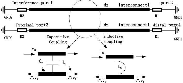
As shown in Fig. 1, there were two independent branch currents from the capacitive coupling current on interconnecting 2:
If Eqs. (3) and (2) were substituted into Eq. (1) to get the computing formula:
2.2. Analysis of distributed RLGC model parameters
Normally, when the low frequency signal was transmitted, the distribution parameters of interconnects need not be considered; When high frequency signal was transmitted or being radiated by high frequency and high energy signals (the frequency was about 30 MHz or more, including microwave frequency band), the electromagnetic effect of parallel crosstalk interconnects would generate circuit distribution parameters, as shown in Fig. 2. The equivalent circuit models of lossless crosstalk coupled interconnect were shown in the follow.
Fig. 2Two equivalent circuit models of lossless crosstalk coupled interconnects
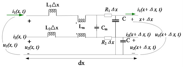
According to Kirchhoff’s law of voltage, the DC resistance voltage divider in high frequency range was neglected. The voltage equations of metal interconnect 1 and interconnect 2 of substrate was as follows:
Similarly, by applying Kirchhoff’s current law, it could be seen that the DC resistance voltage divider in the high frequency range was neglected, and the current equations of the metal interconnects 1 and 2 on the substrates were as follows:
=-jω[(C+Cm)v1(x)-Cmv2(x)]dx,
=-jω[(C+Cm)v2(x)-Cmv1(x)]dx,
where, L was the unit length inductance, Lm was the unit interconnection coupled inductance, C was the unit capacitance of interconnects, Cm was the unit length coupling capacitance of between interconnects. Then the Eqs. (6-9) could be written in matrix form respectively:
Then:
Then:
If the differential of the Eq. (9) and the Eq. (10) was calculated on both sides, there would have the Eq. (11):
So all the analytic results indicated that the reasonable equivalent circuit could substantially show the impacts of these parasitic capacitances, the attenuation of signal, the noise signal and coupling signal.
3. Verification and discussion of crosstalk characteristics of parallel interconnect RLGC model
In the paper, there was constructed the model of micron-level parallel crosstalk interconnections based on FR4 substrate as shown in Fig. 3. There were three important structural parameters of the interconnections, including the width W parameter, the length L parameter, and the spacing S parameter.
The crosstalk intensity was analyzed by FDTD method between parallel interconnects of integrated circuits in Fig. 3. The thickness of semiconductor substrates was 800 um, and insulating layers were 0.58 um, the thickness of interconnect was 35 um, the relative dielectric constants were 4.4 respectively. Considering the symmetry of the structure, a magnetic wall was set on the y= 0 symmetry plane and only the region of y>0 was calculated to reduce the calculation by half thus.
Fig. 3Crosstalk physics simulation model of two parallel interconnects (FR4)

3.1. Near and far end of crosstalk strength structure interconnects
When the spacing D of two interconnects was adjusted to 1W, 3W, 5W and 7W, and other parameters remained unchanged, and the crosstalk intensity varied with the spacing of two parallel interconnects as shown in the Fig. 4 and Fig. 5.
Fig. 4Crosstalk intensity varying with two parallel interconnects spacing
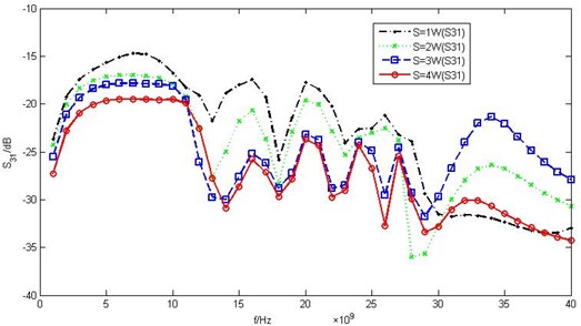
It could be showed from both charts that a linearly increasing trend was increased of the intensity of near-end crosstalk S31 and far-end crosstalk S41 at low frequencies. When the frequency exceeded 10 GHz, there were periodic oscillations with the increase frequency, and the rapid rise of far-end crosstalk S41 was the main factor.
At the same time, when the interconnect spacing increased, the trend of crosstalk change remained unchanged, but the intensity of crosstalk decreased gradually. Obviously, when the line spacing exceeds three times the line width, the far-end crosstalk and the near-end crosstalk do not change much. This showed that the line spacing was no longer the main factor affecting crosstalk, so the interconnect spacing should be increased to three times as much as possible in the design.
Fig. 5Physical test of crosstalk intensity varying with interconnect spacing
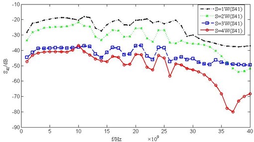
Fig. 6Crosstalk intensity varies with interconnect length
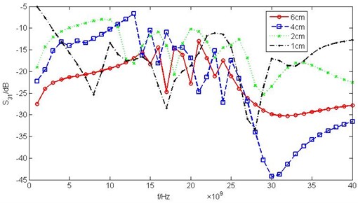
a) Near-end crosstalk S31 varies with interconnect length
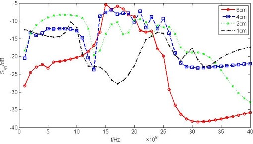
b) Far-end crosstalk S41 varies with interconnect length
3.2. Crosstalk intensity varied with interconnect length
As the interconnect width W=100 um and the interconnect spacing S= 100 um, the crosstalk intensity would change as the interconnect length L was 1 cm, 2 cm, 4 cm and 6 cm, respectively, as shown in the Fig. 6(a) As could be seen from Fig. 6(b), the crosstalk intensity increased with the length of interconnect, and for all length of interconnect, with the increase of frequency, the crosstalk intensity presented a “periodic oscillation” characteristic.
In addition, it could be seen from Fig. 6(a) that the longer the interconnect, the higher the oscillation frequency of the near-end crosstalk; from Fig. 6(b), it could be seen that the longer the interconnect, the greater the oscillation amplitude of the near-end crosstalk. Therefore, planning the design of RF circuits, shorter routes should be used to minimize the length of routes.
4. Conclusions
In the paper, the laws of physics were studied on the model of micron-level crosstalk interconnections, which was constructed based on FR4 substrate. It was completed a series of simulation experiments and physical experiments by changing the input variables of the length and the spacing. With the increase of the length of the interconnect, the crosstalk intensity of the proximal end and the distal end increased. When the interconnect spacing increased, the trend of crosstalk was not changed, but the intensity decreased gradually. The simulation data was consistent with the experimental data to show that the crosstalk interconnections model was accuracy and high efficiency.
References
-
Huang W., Chen C., Lu C., et al. A novel design to prevent crosstalk. TENCON 2007 – 2007 IEEE Region 10 Conference, Taipei, 2007, p. 334-337.
-
Duan C., Calle V. H., Khatri S. P. Efficient on-chip crosstalk avoidance CODEC design. IEEE Transactions on VLSI systems, Vol. 17, Issue 4, 2009, p. 551-560.
-
Gonzalez O., Jose A. P., Herrera A. An extension of the lumped-network FDTD method to linear two-port lumped circuits. IEEE transactions on Microwave Theory and Techniques, Vol. 54, Issue 7, 2006, p. 3045-3051.
-
Berenger J. P. Long range propagation of lightning pulses using the FDTD method. IEEE Transactions on Electromagnetic Compatibility, Vol. 47, Issue 4, 2005, p. 1008-1011.
-
Young B. Digital Signal Integrity: Modeling and Simulation with Interconnects and Packages. Prentice Hall, London, 2001.
-
Chen J. H., Niu Z. Q. Effect of guard trace on signal integrity and coupling noise of microstrips with different parameters. Chinese Journal of Radio Science, Vol. 25, Issue 1, 2010, p. 53-58.
-
Ei Tanani M.-A., Rebeiz G. M. Corrugated microstrip coupled lines for constant absolute bandwidth tunable filters. IEEE Transactions on Microwave Theory and Techniques, Vol. 58, Issue 2010, 2010, p. 956-963.
-
Berenger J. P. Perfectly matched layer for the FDTD solution of wave-structure interaction problem. IEEE Transactions on Antennas Propagate, Vol. 44, Issue 1, 1996, p. 110-117.
-
Zeng R., Kang P., Zhang B., et al. Lightning transient performances analysis of substation based on complete transmission line model of power network and grounding systems. IEEE Transactions on Magnetics, Vol. 24, Issue 4, 2006, p. 875-878.
-
Dai F. Scattering and transmission matrix representations of multi-guide junctions. IEEE Transactions on Microwave Theory and Techniques, Vol. 40, Issue 7, 1992, p. 1538-1544.
-
Liu Xin Hong Dual-mode Band pass Filter Using Stub interconnect-Loaded Interconnect. Journal of Radio Engineering, Vol. 46, Issue 3, 2016, p. 62-64.
-
Hall S. H., Heck H. L. Advanced Signal Integrity for High-Speed Digital Designs. John Wiley and Sons, 2009.
