Abstract
In recent years, intensive development of field-effect transistors on metal-ferroelectric-semiconductor for use, as non-volatile memory elements. The principle of operation of these devices is as follows. Ferroelectric film contains a large number of domains, having a certain vector of electric polarization. Total polarization of the individual domains gives spontaneous (spontaneous) polarization film (non-zero resultant dipole moment per unit volume of the sample). Module and spatial orientation of the spontaneous polarization can be changed under the influence of an external electric field. In strong fields, the film becomes a single-domain. The application of a strong electric field in opposite directions on a certain part of the surface can lead to a reversal of the ferroelectric domains of the film within this area that lends itself to registration. Thus, the effect of polarization in ferroelectric films allows you to create non-volatile memory devices, data carriers which are the domain reversal. These devices have several advantages over traditionally used magnetic and optical data carriers. The purpose of this paper is to study the possibility of using ferroelectric films of complex oxides deposited on original technology on a silicon substrate as a recording media storage devices for external storage.
1. Introduction
Experimental technique. It is known that the physical properties of ferroelectric films are dependent on the state of the surface and the surface of the silicon substrate, stoichiometry, crystallinity, density, microstructure, crystallographic orientation, and the presence of structural defects, and therefore, the methods of producing films [1, 2]. This leads, on the one hand, substantial differences in the parameters of massive and film ferroelectrics, and on the other – to the widely varying characteristics of the films themselves [2, 3].
The basic requirements for thin ferroelectric films: 1) the film and the substrate were approximately the same coefficient of thermal expansion, and 2) the material of the film was characterized by good adhesion to the substrate, and 3) the memory effect was significant. Satisfy these requirements materials like PbTiO3, BST. The substrate to be coated studied film discs were used from a single crystal of silicon.
When growing thin films of complex oxides should be considered a determining influence on the degree of ordering of the structure of vacuum condensates temperature of the silicon substrate, especially with a reactive and volatile components (such as lead). [1] Therefore, the optimal process conditions obtaining ferroelectric films of complex oxides selected by varying the temperature of the silicon substrate, the oxygen pressure in the vacuum chamber and the distance between the target and the substrate of silicon.
Metal thin film composition was prepared by magnetron sputtering of metal layers of Ti and Pb from two separate magnetrons in a single process cycle with prior vacuum in the chamber to a pressure P = 0.25 Pa. As used argon gas atomization. The deposition rate of titanium at the operating pressure P = 0.16 Pa, anode current of I = 0.5 A was 0.35 nm/s, the deposition rate of lead at P = 0.27 Pa, the I = 0.2 A was 2.5 nm/s. Separate deposition of metals allowed to form the structures required thickness with different sequence of metal layers. The substrates used single-crystal Si (100). The objects of the study were two types of thin-film structures (Pb/Ti/Si and Ti/Pb/Si) with thicknesses of the metal layers of ~ 500 nm. Heat treatment of thin-film lead-titanium (Ti-lead) was carried out in a quartz reactor furnace heating resistor with T1 = 450 K and T2 = 950 K with the duration of each stage of annealing, equal to 15 min at a flow rate of oxygen 35 l / h. The thickness of the grown films was monitored by microinterferometer MI-4 and was 400 ± 50 nm.
Relative permittivity ε sample ferroelectric films were determined by the known method [3, 4] on the bridge tanks E8-2 using an external oscillator (LF generator G3-33) and the null indicator F582. The measurement field was chosen for reasons of minimally acceptable sensitivity and noise immunity. Measurements were carried out at a frequency meter field 1000 Hz.
Мeasurement procedure. We used four-vacuum magnetron sputtering coating plant multilayer and multicomponent films. The unit provides an different processes of film deposition thickness 0.1-5 μm in diameter on the substrate 60-200 mm, as well as square or rectangular with linear dimensions of 30-200 mm. The unit has four operating positions: locking and heating, ion cleaning of the surface of substrates, magnetron sputtering target materials of the three small diameter. The deposition of multi-component (ternary) films - septum removed, spraying is carried out simultaneously with the three targets of different materials. By controlling the supply of power to each target changes the content of the material components in the deposited film.
The phase composition of the films was determined by X-ray diffraction on a DRON-3M (radiation CuKα) in the angular range 20-65°. The surface morphology of the films and the film-substrate were observed using scanning electron microscopy. To measure the electrical properties of the films by magnetron sputtering in a vacuum through a mask with holes 1 mm was applied to the upper nickel electrode, the lower contact to the silicon wafer was carried indium-gallium eutectic. Dielectric hysteresis loops measured at a voltage of 0.5 V and a measuring frequency of 50 Hz.
Diffraction patterns of the films were determined by the unit cell parameter (the splitting of the peak corresponding to the spontaneous strain is not observed), the type of texture, size mikrodeformation Ad/d (where d – the distance between planes) and the size of the coherent scattering D. The accuracy of the unit cell parameter was limited by the width of reflections and was ±0.0003 nm. Type of texture (preferred orientation of the crystalfishing) was estimated by the deviation of the relative intensities of the reflections of the standard (polycrystalline). Structural and strain characteristics Ad/d and D, traditional radiography [5], were used to describe the quality of the crystallization of the films. The values of Ad/d and D from the widths of X-ray reflections is a standard method of approximations [6]. Error in determining the Ad/d and D did not exceed 15 % and 30 %, respectively. Method cannot set the size of coherent scattering of less than 100 nm.
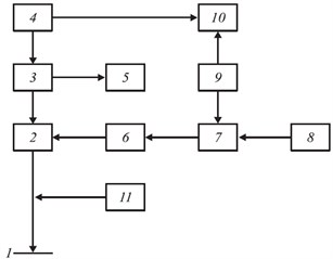
The current-voltage characteristics of the structures were removed in accordance with the methodology described in [7], the use of electrostatic probe on the bench, the circuit is shown in Fig. 1. The probe was used specially prepared by electrochemical grinding tungsten wire probe tip with a radius of curvature of 0.5 ± 0.03 μm. This parameter controls the probe was carried out using microinterferometer MI-4.
To control the reproducibility of the ferroelectric properties of complex oxide films deposited on silicon substrates, the current-voltage characteristics were recorded in three arbitrary points located at different distances from the center of the silicon wafer.
The resolution of the structures determined by the following method [7]. Mounted on the test stand (Fig. 1), the sample was moved in steps of 0.4 μm relatively tungsten probe. Movement of the sample was monitored with the help of the reference-measurement system with vacuum tube transmitter. The recording process is supplying the probe pulse voltage U = ± 80 V. The presence of the recorded information was determined by measuring the deviation of the oscillator frequency reproduction with a frequency FS-63/3 when the sample is moved in steps of 0.1 μm to starting position. The results of measurements plotted deviation oscillator frequency playback of moving the sample relative to the tungsten probe.
Speed reversal of studied ferroelectric films was determined according to the methods proposed by Metz [8].
Fig. 1Block diagram of the measuring stand: 1 – drive to the probe record-playback, 2 – key switching record-playback, 3 – generator play (20 ≤ ν ≤ 50 MHz), 4 – power supply generator B5-47 (0-15V), 5 – RW-frequency 63/3, 6 – key changes the polarity of the pulse, 7 – pulse amplifier, 8 – generator G6-25, 9 – DC power supply B5-3050, 10 – unit combined digital SCH4313, 11 – exact positioning unit (step 0.1 μm)
2. Results and Discussion
In the investigation of the temperature dependence of the relative permittivity of the films of complex oxides obtained on silicon substrates, was found maximum on the ε(T) in the expected temperature of the ferroelectric phase transition of bulk materials [3] (Fig. 2). However, this maximum is negligible and smeared over a wide temperature range. Diffraction patterns of the structures are shown in Fig. 3.
Fig. 3X-ray diffraction study of materials: a – single crystal silicon (slice (100)), b, c – composite insulator-silicon oxide-silicon (0.4 μm thickness of the dielectric and 0.6 μm, respectively)
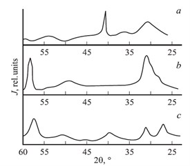
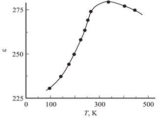
Fig. 2.εT
In Fig. 3a survey shows the results of a single crystal of silicon (the cut (100)). He recorded the reflection from the (200) with an angle of 2θ = 41.9° and a group of lines in the corners of, 30-31° belonging to unidentified compounds of silicon (presumably SiO2 – α-quartz; SiO).
In Fig. 3b shows diffraction patterns of composition insulator-silicon oxide-silicon. Dielectric film is highly textured (there is only one reflection). 2θ = 57.2° diffraction peak in the region corresponding to the oxides of silicon, much more intense, indicating an increase in the thickness of the oxide layer. The orientation of the crystallographic direction of the film faces is different from the orientation of the (100) silicon, so the reflection from the (200) silicon is absent. The film is thin (about 0.5 μm). Increased background can be explained by the fact that the film is in the process of coalescence.
Fig. 3c corresponds to a structure similar to pretax shown in Fig. 3b, but in this case the ferroelectric film has a thickness of 5.3 μm. The presence of reflections from the (100) (110) (200) indicates an increase in release texture.
Results of the determination of the current-voltage characteristics obtained in three arbitrary points of the studied samples are shown in Fig. 4.
Fig. 4The current-voltage characteristics obtained in three arbitrary points of the sample
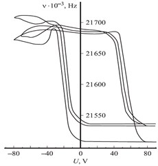
Fig. 5The results of the measurement resolution of the structures
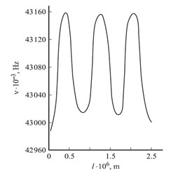
Fig. 6Time dependences applied electric voltage U and current I
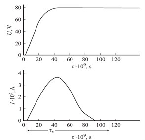
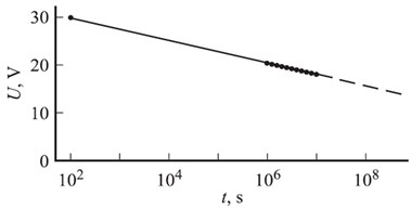
Fig. 7The time variation of the amplitude of the electrical signal from the time
These data show that the change in the capacitance of the sprayed layer reaches 0.01-0.02 pF (measured in units of 25-35 kHz). Amplitude change recorders area studied sample due to: 1) the thickness of the in homogeneity, and hence the capacity of the deposited dielectric layer, and 2) the uneven distribution of structural defects that reduce the degree of ordering of the film structure, and 3) with the heterogeneity of the elastic fields of mechanical stress on the film thickness, arising from the uneven heating of the silicon substrate in the formation of complex oxide films. These causes are caused by technological problems that can be resolved with the appropriate tooling and completion modes produce films of complex oxides. Change in the capacitance of the depletion layer of silicon, compared to the change capacity deposited film, it was very small (no more than 0.003 pF) and virtually no effect on the memory effect.
A plot of the frequency deviation of the generator play from moving the sample with respect to tungsten probe is shown in Fig. 5. The experiment showed that the resolution of the structures when they interact with a tungsten probe having a radius of curvature of the tip 0.4 μm, no worse than 0.7 μm, which points to the real possibility of achieving density recording 1012-1013 bit/m2.
The results of determining the rate of depolarization of the investigated films of complex oxides are shown in Fig. 6. The data indicate that the switching of domains in ferroelectric films studied amounts of less than 100 ns.
Reproduced signal amplitude change with time obeys the logarithmic law (Figure 7). Extrapolation according to the region of large times shows that in 10 years (t ≈ 3∙108 s) store information reproduced signal amplitude is more than 50 % of the initial value, which is a satisfactory result for the recording media, volatile media.
3. Conclusions
From these data it follows that of the film, at least, to a thickness of 0.5 μm has a perovskite structure, and the material of the film is highly textured.
Shown in Fig. 3, the data are ordered disordered crystal film with the highest degree of crystallization, which is characterized by the following values of the structural deformation parameters: the size of the coherent scattering of D > 100 nm; magnitude micro strain Ad/d ~ 0.01. The degree of ordering of the film structure can be varied by changing the temperature of the silicon substrate. In particular, the decrease of the temperature leads to a disordered structure. Further studies of the properties of complex oxide films grown at different temperatures silicon wafers showed that the process of disordering of the structure of films accompanied by degradation of their ferroelectric properties. The values of the coercive field and spontaneous polarization of the films thickness 2000-2500 nm were: Ec = 4.5 kV/cm, Ps = 16.2 μC/cm2. Electrophysical studies of the structures shown in principle can be used as recording media storage devices for external storage.
References
-
Vorotilov K. A., Muhortov V. M., Sigov A. S. Integrated Segnetoelectric Devices. Edited by the Corresponding Member of the Russian Academy of Sciences Sigov A. S., Moscow, Energoatomizdat Publishing House, 2011, 175 p., (in Russian).
-
Afanasyev M. S., Burov A. V., Yegorov V. K., Luchnikov P. A., Chuchyova G. V. Pecularities of ror-spectroscopy of thin films of perovskytes. Herald of Science of Siberia, Vol. 1(2), 2012, p. 126-133, (in Russian).
-
Myasnikov E. N., Tolstouchov S. V., Frolenkov K. Yu Memory effect in segnetoelectric films BST on the basis of cremnium. Physics of Rigid Body, Vol. 46, Issue 12, Moscow, 2004, p. 2193-2199, (in Russian).
-
Muhortov V. M., Yuzyuk Yu. I. Heterostructures on the Basis of Nanosized Segnetoelectric Films: Obtaining, Qualities and Application. Rostov on Don, Southern Scientific Center of the Russian Academy of Sciences, 2008, 224 p., (in Russian).
-
Klyeto G. I., Martyniuk Ya. V., Savchyuk A. I., Stryebyezhov V. N., Obiedzinskiy Yu. K. Nanosized segnetoelectric films for integral memory elements. Nanosystems, Nanomaterials, Nanotechnologies, Vol. 7, Issue 1, 2009, p. 65-71, (in Russian).
-
Sidorkin A. S., Nesterenko L. P., Smirnov A. L., Smirnov G. L., Sidorkin A. A., Ryabtsev S. V. Parameters of domain boundaries in thin PbTiO3 films. Ferroelectrics, Vol. 359, Number 1-6, 2007.
-
Zhou X. Y., Heindl T. H., Pang G. K., Miao J., Zheng R. K., Chan H. L. W., Choy C. L., Wang Y. Microstructure and enhanced in-plane ferroelectricity of Ba0.7Sr0.3TiO3 thin films grown on MgAl2O4 (001) single-crystal substrate. Appl. Phys. Lett., Vol. 89, 2006, p. 1-3.
-
Wang S. Y., Cheng B. L., Wang C., Dai S. Y., Jin K. J., Zhou Y. L., Lu H. B., Chen Z. H., Yang G. Z. Raman spectroscopy studies of Ce-doping effects on Ba0.5Sr0.5TiO3 thin films. J. Appl. Phys., Vol. 99, 2006, p. 1-6.
-
Weller S. T. Dielectric and structural properties of pulsed laser deposited and sputtered barium strontium titanate thin films. Mater. Sci. Eng. B, Vol. 139, 2007, p. 177-185.
About this article
This research is funded by the European Social Fund under the Project "Microsensors, Microactuators and Controllers for Mechatronic Systems (Go-Smart)" (Agreement No VP1-3.1-ŠMM-08-K-01-015).
