Abstract
This work proposed a binary-weighted Digital-to-Analog Converter (DAC), which is designed to be used in Asynchronous successive approximation register (SAR) based Analog-to-digital converters (ADCs) specifically and in other relevant operations .The design has yielded an improved slew rate, and it is less prone to noise as the size of capacitors is taken in accordance with KT/C noise calculation. For achieving all mentioned goals, and to restrict the size of DAC, within suitable dimensions charge scaling DACs are used. One more advantage of this design is its accuracy, further it does not require op-Amps for its operation. Results of statistical simulation and mathematical consideration are published which depicts the supremacy of the design. A high-resolution DAC designed for this specific purpose has to have special consideration for the effect of local mismatch, parasitic and matching of the capacitors, for that, the common-centroid approach has been followed. This design has displayed a high resolution with small unit capacitances and that too without expensive factory calibration.
Highlights
- The effect of KT/C noise is limited in the designing of Digital to Analog Converter (DAC).
- The size of unit capacitor in the designing of binary weighted DAC is crucial and responsible for noise and other deviations.
- The settling time of the DAC needs to be as low as possible for the better performance of the DAC, and can be controlled by taking due measures of the parameters.
1. Introduction
1.1. Asynchronous SAR ADC Principle
A very basic form of Asynchronous SAR ADC consists of five blocks namely, a Sample and Hold (S/H) Circuit, a Comparator, an asynchronous logic block, a Successive Approximation (SA) Register and a DAC. In the conventional SAR ADCs, due to comparator metastability, the time period of external clock is kept to give sufficient time to comparator even for the worst case of comparison [1].
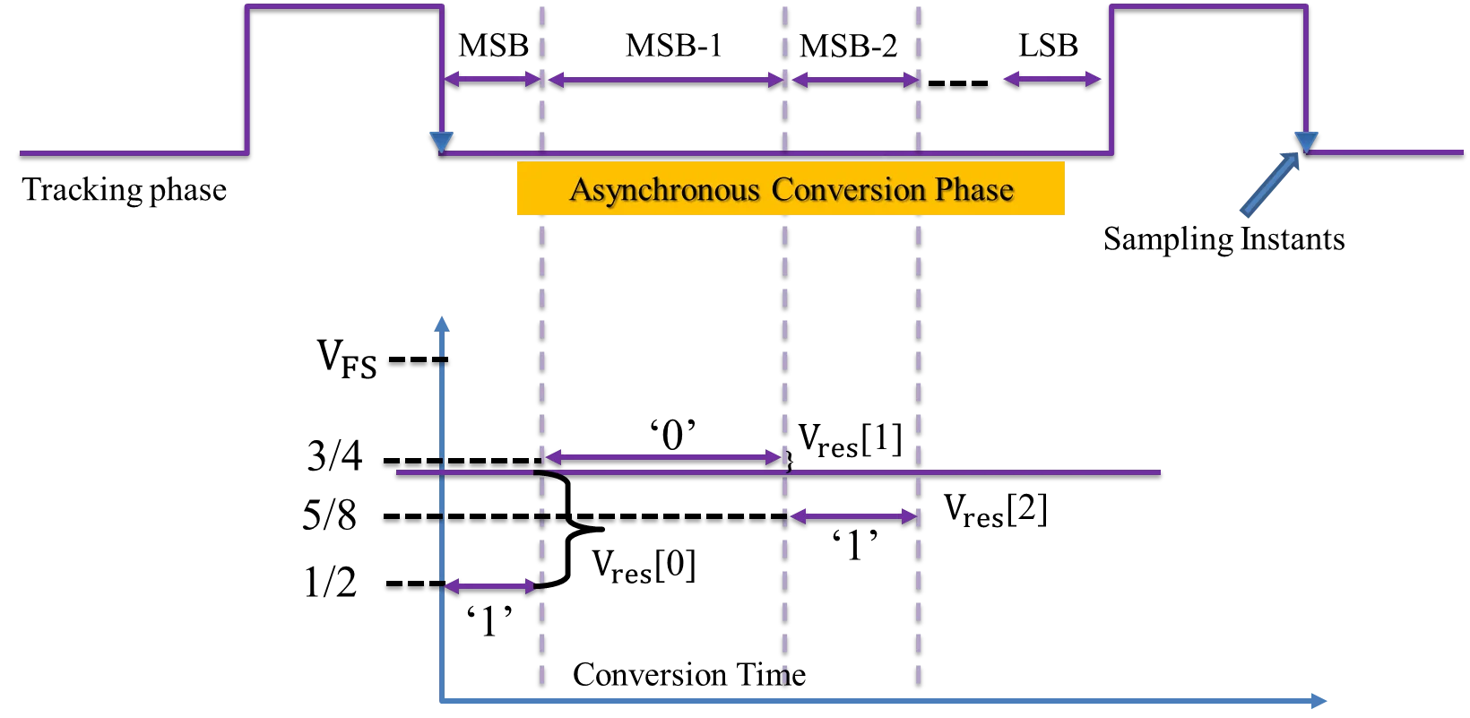
In asynchronous operation, it is intended that this overhead time is reduced or vanished. This is possible if comparator instead of waiting for the next clock edge will generate its own clock to trigger SA register for next level of comparison.
Fig. 1 demonstrates the concept involved in asynchronous data processing in SAR ADC. As it can be seen that no fixed amount of time is dedicated to each conversion step; instead, comparison time is made to vary in amount depending upon the comparator resolving time. In this way, asynchronous processing speeds up to the overall rate of conversion of ADC.
For adapting these changes each sub-block of conventional SAR-ADC is to be configured. The proposed work focuses on the modification of DAC. In asynchronous operation, although a finite time will remain associated with DAC settling, the resolving time for the comparator is no longer fixed. So, in its architecture, the DAC settling time starts immediately after the comparison is done. The time elapsed by the comparator's comparison varies from case to case. This is how the ADC can produce an output as soon as a bit is decided. This can also reduce the overhead time required for the conversion and thereby increases speed.
Fig. 1Asynchronous operation [1]
![Asynchronous operation [1]](https://static-01.extrica.com/articles/21523/21523-img1.jpg)
1.2. Background and motivation
Binary weighted DAC [2] are widely used in wideband applications, it is also a key building block of the asynchronous SAR-ADC [3-5], which is rapidly gaining popularity because of its high-speed. In all these applications, settling time of the DAC often limits the speed of operation. Hence leads a requirement of improving the settling time [6].
Further to reduce the size of DAC, various placement methods of the capacitive array have been reported. For example, the heuristic search approach, intended to increase the degree of depressiveness in the layout but the placement might not have a common-centroid arrangement and thus resulting a systematic mismatch [7, 8].
The proposed DAC structure is a tradeoff between speed and area, and that too have a reduced settling time. It combines the features from the Binary weighted DAC and charge-redistribution DAC.
One more approach trading area with speed was proposed by [9]. However, it requires double the area for capacitor, in comparison with the proposed design and requires an operational amplifier (Op-Amp) with a large feedback capacitor for voltage division. Whereas, in the proposed model there is no requirement of Op-Amp. [10].
1.3. Paper structure
The structure of the paper is as follows. In Section 2, Challenges in the designing of DAC and in calibration of capacitor size are discussed. Based on that a principle for a calibrated structure for the designing of DAC suitable for Asynchronous SAR ADC is discussed. In Section 3 the working of proposed model is explained. In Section 4 the schematic of the proposed design is presented, and with the help of Tanner EDA tools layout of the proposed design is drawn, and simulation results are obtained. In the last section, the transfer function of the proposed DAC is represented, and paper is concluded.
2. Challenges in the designing of DAC and in calibration of capacitor size.
In designing process, the small size of capacitor is always desirable because it will reduce the area of the device, consumes less power, and will result in a fast conversion. Along with large number of capacitors are required for achieving high resolution, and in that case voltage accuracy will become more critical and that depends on the capacitance. Further, there are challenges associated with the smaller capacitance like KT/C noise and mismatch.
2.1. KT/C noise
KT/C noise represents a particular case of thermal noise of a resistor and generally result from the low pass filter formed by parasitic resistance and capacitor and is given by Eq. (1):
As it can be seen from Eq. (2), that the noise is independent of resistance and inversely proportional to the value of capacitance. This value of capacitance is the accumulative value of all the capacitance present in the DAC:
where, is representing the unit capacitance. For reasonable and acceptable operation of DAC the KT/C noise should be less than the least significant bit, and generally assumed to be the half of the value of , Hence:
From the Eq. (3), the value of resolution can be written as a function of as:
The relationship presented in Eq. (4) is plotted in Fig. 2 that depicts, KT/C noise is not the limiting problem for DCA architecture.
2.2. Matching
Mismatch of the unity cell is generally a reason for non-idealities caused, during the process of production. This majorly includes dielectric thickness and varying capacitor size. Further, the parasitic of the capacitors and even there wiring can affect the capacitance of each unit capacitor. All these effects can be described using a single term “capacitance standard variation” if normal distributions of the capacitors are assumed. The important point is to note that if one chooses increasing capacitance, e.g. common centroid approach, as in this case, this decreases due to law of area according to the Eq. (5):
where, is technology-specific constant.
3. Theoretical analysis and development
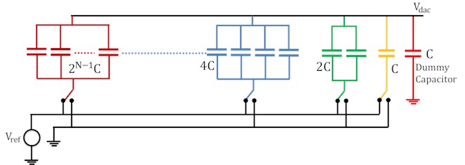
The implemented Capacitive DAC used in Asynchronous SAR ADC design is shown in Fig. 4 and Fig. 7 the proposed work have used two different configurations, namely, the Binary-Weighted Capacitive DAC and the charge scaling Capacitive DAC using combination of two 4 bit charge scaling DAC.
Fig. 2Achievable resolution for conventional CSA architectures due to kT/C noise, T= 300 K [11]
![Achievable resolution for conventional CSA architectures due to kT/C noise, T= 300 K [11]](https://static-01.extrica.com/articles/21523/21523-img2.jpg)
The architecture of Binary Weighted Capacitive DAC comprises of parallel connected capacitors [12] without any Op-Amp. The output of DAC is given by:
where, is the analog output voltage, is the reference voltage, is the factor and is the digital word given by equation:
where, is the number of bits of the digital word,
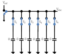
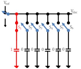
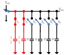
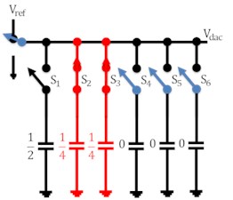
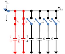
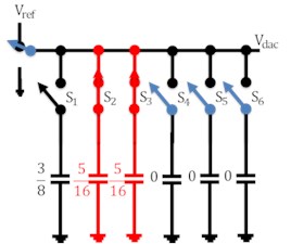
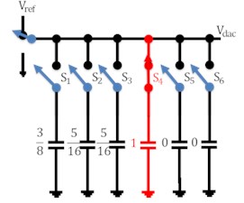
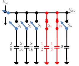
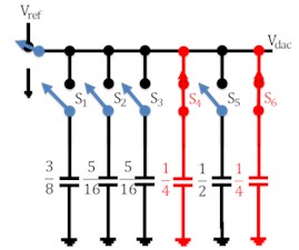
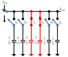
The working of the capacitive DAC array of 5 bit is shown in Fig. 3 in which charging and discharging of capacitor is involved. For simplicity analog input voltage has been taken as 0.34 V while reference voltage as 1.2 V. In the reset phase all the capacitors are connected through ground so as to nullify charge in them. When the switch is connected to voltage i.e. in the sampling phase, capacitor switch s1 is made to turn ON so that this capacitor is charged by voltage while other capacitors switches remained disconnected. In the next phase, switches s1 and s2 of capacitors C1 and C2 respectively are closed as shown in Fig. 3(c). These capacitors are now charged by /2. Comparator compares the applied analog input voltage value with analog output of DAC. Comparator gives the output as logic 1 if and vice versa. In the next state, capacitor C1 is made to disconnect from switch s1 and capacitor c2 and c3 are now connected through switches to charge them /4 individually. In this way, corresponding steps are iterated with new clock cycle.
4. Design and development
4.1. Capacitive DAC Schematic (BWC)
The binary weighted capacitors are employed to make a Capacitive Digital-to-Analog converter. Fig. 4 shows the DAC circuit diagram as used in ADC. In the case of binary weighted capacitive DAC the value of each capacitor leg increases from C to C on moving from LSB to MSB. Out of various available options to implement DAC the chosen approach yields most accurate design. Also, it does not require op-amps for its operation.
Fig. 3Working of DAC
a)
b)
c)
d)
e)
f)
g)
h)
i)
j)
Again, capacitive DAs are of various types but only binary weighted configuration is chosen because of its linearity of output. Also, the value of unit capacitor used in DAC is chosen to be 17.6fF so as to minimize the effect of thermal noise.
Capacitors are easier to fabricate and far more accurately reproduced with respect to resistors. Area of capacitors cannot be taken very large because this with increase overall area of DAC and hence area of ADC. Lower limit of capacitor area is decided by thermal noise value (KT/C). This noise should not be greater than half of the LSB for proper functioning of DAC.
CDAC cannot give precise output voltage as it is expected because of the unavoidable manufacture induced capacitor mismatch. As the capacitor size increases capacitor mismatch decreases. Capacitor mismatch is inversely proportional to the square root of area. A large value unit capacitor is generally demanded to keep capacitor mismatch down. Therefore, the unit capacitor value in the Asynchronous SAR ADC has been taken larger than what is expected by the kT/C (thermal) noise calculation. Large capacitors not only engage more chip area, but it also costs more power to switch the capacitors between Vref and the ground. So, a moderate value of capacitance has been chosen and 17.6fF unit capacitor is used for CDAC. This capacitor size is decided so as to keep KT/C (thermal) noise within half LSB limits.
Fig. 4BWC DAC schematic
4.2. Capacitive DAC layout (BWC)
The layout of 8 bit Capacitive DAC has been sketched in L-Edit SCN3ME_SUBM 0.5 um technology and shown in Fig. 5. The common centroid approach is followed to design the layout of Capacitive DAC [13]. In order to suppress effects of systematic mismatch [14, 15] and to achieve least mismatch among repetitive structures, designers usually choose a common-centroid layout structure [16].
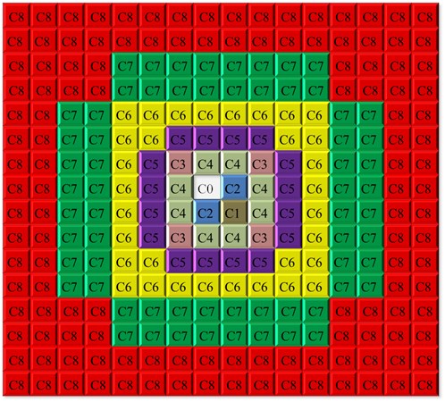
In common-centroid distribution, it is intended that the center of each capacitor leg (which is made up of unit capacitors of 17.6fF value) must either coincide or lie as close as possible with a common center of whole DAC. This brings out symmetry in the design and hence reduces symmetrical error. In the Fig. 5 distribution of unit caps over the whole area of DAC has been shown. Here a unit capacitor is referred to as ‘C’ with its suffix denoting the leg to which it belongs. For example, unit capacitor C5 (5) belongs to 5th leg of DAC and is a part of 24 = 16 capacitors in that leg.
The value of each unit capacitor of charge scaling CDAC is 17.6fF which is in agreement with KT/C noise calculation and the values of capacitors from LSB to MSB vary in multiple of 17.6fF. The type of capacitors used in CDAC layout is double polysilicon capacitor [17]. In Fig. 6 capacitor C0 is dummy capacitor while other capacitors from C1 through C8 are for LSB to MSB respectively. The capacitance per unit area of poly-poly2 overlap in AMI 0.5 m technology is 950 aF/m2 [18].
Fig. 5BWC DAC layout
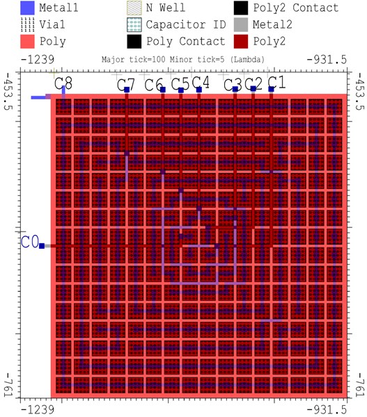
Fig. 6Unit capacitor distribution in DAC
4.3. Capacitive DAC schematic (using Sub DACs)
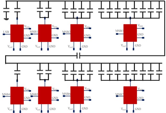
Although the Binary Weighted Capacitive DAC had various advantages but in order to reduce more area of ADC, Implementation is carried out using another type of DAC. This implemented DAC is made up of two 4 bit charge-scaling subDAC [17].
The schematic of this DAC is shown in Fig. 7. Note that value of scaling capacitor is very critical in deciding the linearity of output characteristics of this DAC.
The value of scaling capacitor has been kept so that the LSB array can terminate the MSB array with an equivalent capacitance of . Mathematically it can be found that:
where is value of scaling capacitor and is unit capacitor [17].
Fig. 7DAC Schematic using two 4 bit subDACs
4.4. Capacitive DAC layout (using subDACs)
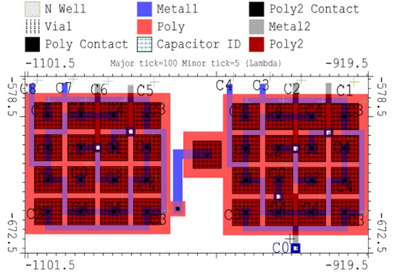
Similar approach has been followed in designing the layout of this 8 bit DAC. Common centroid structure of a 4-bit DAC has been used in this layout as shown in Fig. 8.
Fig. 8DAC Layout using two 4 bit subDACs
4.5. DAC switch schematic and layout
Switches are connected to all unit capacitors from MSB to LSB and are used to charge or discharge the capacitors according to control voltage. This control voltage, applied individually to each capacitor-leg switch is governed by digital output of SA register.
Fig. 9Schematic of switch
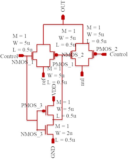
Fig. 10Layout of switch
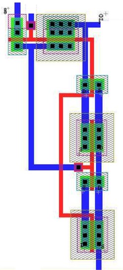
As shown in Fig. 9, the switch used for DAC switching operation has been implemented using two simple transmission gates. The control voltage has been applied to decide whether connect or disconnect a particular capacitor leg from reference voltage applied to DAC. If control voltage is HIGH then, OUT node get connected to reference voltage applied, and if it is LOW, then OUT node get connected to ground. Fig. 10 represents the layout of switch.
5. Simulation result of capacitive DAC
5.1. Transient analysis
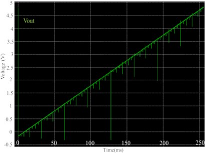
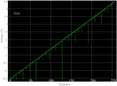
Fig. 11 shows the transient response of the proposed DAC, Fig. 11(a) shows the transient response of 8 bit Binary Weighted Capacitive DAC and Fig. 11(b) is showing the transient response of another designed in which 8-bit DAC is made up of two 4 bit charge-scaling subDAC. The layout of both the designs were drawn using S-Edit of Tanner EDA and the simulation results were obtained using T-Spice. The implementation was carried out in a 0.5 μm CMOS Technology. The DAC is subjected to all the possible digital inputs starting from [00000000] to [11111111]. The reference voltage applied to DAC is 5 V. The size of unit capacitor used is chosen as 17.6fF that is in accordance with the KT/C noise ratio. As can be seen from both the figures that transition is almost same whether one uses subscaling DAC or Binary weighted DAC where they are different from designing point of view. One can use any of the proposed architecture depending on the availability of the space.
Fig. 11Transient analysis
a) BWC DAC output waveform
b) DAC using subDAC output waveform
5.2. DNL and INL plot
Fig. 12 is showing the differential nonlinearity (DNL) and integral nonlinearity (INL) plot corresponding to the transients depicted in Fig. 11. The INL and DNL plot was drawn to check the nonlinearity errors and that happen to be less than ±0.6 LSB, that make the proposed DAC more significant.
Fig. 12DNL and INL plot
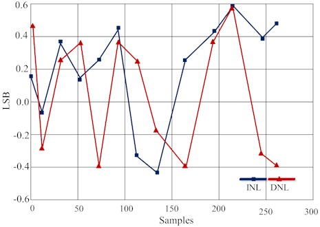
Fig. 13DAC settling
5.3. Settling time
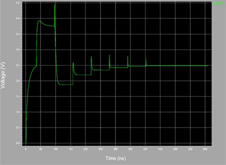
Fig. 13 shows the Settling time in data conversion system plays very important role as various analog operations follow a sequence and completion of the preceding state must be ensured before the starting of next state. By definition, it’s the time required by the converter to settle for its final output value and it should be as low as possible. In Fig. 13 the settling behaviour of the proposed DAC is shown. The -axis is representing time in Nanosecond and -axis is representing voltage in Volte. As it can be seen from the transitions shown in figure that the proposed approach has achieved a DAC settling of 2.48 V within 400 ns, which is comparatively very less in comparison with the available DACs in the market [19].
6. Conclusions
In the proposed work, its been diagnosed that the effect of KT/C noise is limited in the designing of DAC. Whereas matching plays a crucial rule in designing. Based on that a calibrated value of unit capacitor is chosen and designing of DAC is completed in two different configurations namely BWC and sub-DACs. from the layout of these design using Tanner EDA tool, one can see the area consumed is comparatively less. Transient of both the design is plotted and depicts high resolution and speed when compared with the available designed of DAC for asynchronous SAR ADC. The INL and DNL plot has ensured the linearity of the proposed designed and output settling has shown that the output is settling fast enough to make the design unique and fast. As a future work one may implement the design with SAR-ADC to further ensure the effectiveness of the design.
References
-
Lecture Notes in Networks and Systems, Proceedings of 1st International Conference on Computing, Communications, and Cyber-Security, Vol. 121, Springer Nature, 2020.
-
Zhu Yan, et al. A 10-bit 100-MS/s reference-free SAR ADC in 90 nm CMOS. IEEE Journal of Solid-State Circuits, Vol. 45, Issue 6, 2010, p. 1111-1121.
-
Xu Ruoyu, Bing Liu, Jie Yuan Digitally calibrated 768-kS/s 10-b minimum-size SAR ADC array with dithering. IEEE Journal of Solid-State Circuits, Vol. 47, Issue 9, 2012, p. 2129-2140.
-
Yoshioka Masato, et al. A 10b 50MS/s 820µW SAR ADC with on-chip digital calibration. IEEE International Solid-State Circuits Conference, 2010.
-
Kim Hyo Jong, Seo Donghwan, Lee Byung Geun Settling time optimization technique for binary-weighted digital-to-analog converter. IEICE Electronics Express, Vol. 11, Issue 6, 2014, p. 20140132.
-
Chen Jwu E., Luo Pei Wen, Wey Chin Long Placement optimization for yield improvement of switched-capacitor analog integrated circuits. IEEE Transactions on Computer-Aided Design of Integrated Circuits and Systems, Vol. 29, Issue 2, 2010, p. 313-318.
-
Yongfu Li, et al. Placement for binary-weighted capacitive array in SAR ADC using multiple weighting methods. IEEE Transactions on Computer-Aided Design of Integrated Circuits and Systems, Vol. 33, Issue 9, 2014, p. 1277-1287.
-
Ali Bhat Snober, et al. Dynamic Access Control In Iot: Monitoring User Behavior Using Smart Contracts. 12th International Conference on Electronics, Computers and Artificial Intelligence, 2020.
-
Singh Ritu Raj, et al. Multi-step binary-weighted capacitive digital-to-analog converter architecture. 51st Midwest Symposium on Circuits and Systems, 2008.
-
Mueller Jan Henning, et al. The impact of noise and mismatch on SAR ADCs and a calibratable capacitance array based approach for high resolutions. International Journal of Electronics and Telecommunications, Vol. 59, Issue 2, 2015, p. 161-167.
-
Allen P. E., Holberg D. R. CMOS Analog Circuit Design. 3rd, Oxford University Press, 2011.
-
Lin Cheng Wu, et al. Common-centroid capacitor placement considering systematic and random mismatches in analog integrated circuits. 48th ACM/EDAC/IEEE Design Automation Conference (DAC), 2011.
-
Soares Carlos Fernando T., Antonio Petraglia Automatic placement to improve capacitance matching using a generalized common-centroid layout and spatial correlation optimization. IEEE Transactions on Computer-Aided Design of Integrated Circuits and Systems, Vol. 34, Issue 10, 2015, p. 1691-1695.
-
Khalil Dessouky, et al. Evaluation of capacitor ratios in automated accurate common-centroid capacitor arrays. 6th International Symposium on Quality Electronic Design, 2005.
-
Singh Pradeep Kumar, et al. Futuristic trends in network and communication technologies. 1st International Conference, 2018.
-
Singh P., et al. Futuristic Trends in Networks and Computing Technologies. Communications in Computer and Information Science, Vol. 1206, 2019.
-
Martínez Herrera, Alberto F., Carlos Mex Perera J., Juan Nolazco Flores A. Some Representations of the S-Box of Camellia in GF (((2 2) 2) 2). International Conference on Cryptology and Network Security, Springer, Berlin, Heidelberg, 2012.
-
16- and 20-Bit Voltage DACs, https://www.maximintegrated.com/en/products/analog/data-converters/digital-to-analog-converters/MAX5717.html.
-
Sharma Ashutosh, Mohd Dilshad Ansari, Rajiv Kumar A comparative study of edge detectors in digital image processing. 4th International Conference on Signal Processing, Computing and Control (ISPCC), 2017.
