Abstract
The proposed research involves, a design and implementation of DC source fed improved Dual output Buck-Boost converter for agricultural and industrial applications. It consists of step up and step-down converter, DC-link module. Compared with conventional two converters, the designed system results in reduction of voltage tension across the switches, compact power switches, DC source reckoning and reduced inrush current. DC-link switching is achieved by reduced ripple voltage which results in improved quality of obtained output power. Reduction in switch count makes the system more cost effective. In addition, the motor speed is regulated by PI controller. Brushless DC Motor produce torque ripple and cause mechanical vibration, acoustic noise due to structural imperfectness and control system, to overcome this suppression control method of vibration for brushless DC motor utilizing feedforward compensation with Fourier transform utilizing a vibration signal acquired by an acceleration sensor attached to the motor frame is proposed. A simulation and prototype model of Dual output Buck-Boost converter is developed, and its performance is analysed for various operating conditions.
1. Introduction
1.1. Single stage multiport converter
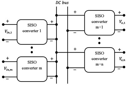
By combating with the challenges of global warming, clean energies, like fuel cell, PV and wind energy have been highly encouraged because of its high their efficiency. Owing to the electrical properties of clean energy, the power generated is severely impacted by the climate or it has transient responses that are slow, and the output voltage is easily affected by load changes [1]. Further, the other auxiliary components, like storage elements, control boards and so on are generally necessary to guarantee the right operation of clean energy [2]. Therefore, different voltage levels are needed in the power converter of a clean energy generation system. Generally, several single input single output (SISO) DC-DC converters with diverse voltage gains are integrated to meet the demands of different voltage levels, such that their system control is more complex and the respective cost is high [3]. The synthesis of multiport converters can be done by connecting different SISO converters to one common dc bus as illustrated in Fig. 1. Though common in traditional hybrid power systems, such kind of configuration can result in a sophisticated structure and huge cost. The inspiration behind the present study is to develop a single input multi output (SIMO) converter for maximizing the conversion efficiency and voltage gain, decreasing the control complexity and helping to save the manufacturing expense of the converter.
SIMO converters can be divided into isolated and non-isolated configurations. In the case of isolated topologies, a transformer with multiple secondary windings acts as an interface between the input and output ports. Only one output voltage generally the one with the heaviest load is controlled while the others are decided by means of the turn ratios of the secondary windings. Therefore, independent output voltage regulation is not a direct impression, and this is not a cost-efficient solution also [4]. The non-isolated SIMO topologies can be further divided into independent- and series-output configurations. With the independent-output configuration [5, 6], every output port shares the same ground and decreases the number of external heavy components like inductors and power switches, resulting in reduced expense and losses in the system. However, in these configurations, loads are constructed independently as illustrated in Fig. 2(a).
Fig. 1Conventional multiport converter architecture
In a similar manner in the series-output configuration [7, 8], as indicated in Figs. 2(b) and (c), various outputs are connected serially. Series regulated DC voltages might be necessary in several low- and high-power applications. One among the most remarkable applications of this new family of DC-DC converters is the boosting and regulation of the low and variable output voltage of renewable energy for the DC link of grid/load connected systems on the basis of inverters. Therefore, Series-output SIMO converters are considered to be effective solutions in balancing the dc-link voltage of loads in an effective manner [9].
Nami et al. [6] have introduced a novel DC–DC multi-output boost converter that can share its total output between the different series of output voltages used in low- and high-power applications. Unluckily, nearly two switches for one output are needed, and DC-DC multi-output control mechanism was complex. In addition, the associated output power cannot provide individual loads in an independent way. Boora et al. [8] also have illustrated a novel multi-output DC-DC converter topology, which has the capabilities of step-up and step-down conversion. In this topology, multiple output voltages could be produced and could be utilized in varied applications like multilevel converters with diode-clamped topology or power supplies with different voltage levels, but the multiple number of switches in the converter results in power losses. Patra et al. [10] have introduced a SIMO DC-DC converter with the capability of producing buck, boost, and inverted outputs simultaneously. Nonetheless, approximately three switches for one output are needed for SIMO.
In addition, in this research paper, we propose a suppression control method for torque vibration of brushless DC motors utilizing the acceleration sensor, the Fourier Transformer and the repetitive controller. In the proposed system, only one frequency component of vibration signal from acceleration sensor is inputted to repetitive controller, the stability of the control system can be improved. Approximate analysis is performed to study the stability of the repetitive control system. In order to realize online generation of feedforward compensation signals to reduce the vibration, auto-tuning method of the repetitive control parameters is also presented.
The periodical torque ripple occurs synchronously with the motor rotation. And also, the repetitive controller has large loop gain (basically infinity) only for the fundamental repetitive frequency component and its harmonics. For the above reasons, the repetitive control system is effective to reduce the vibration due to periodical torque ripples.
Fig. 2Non-isolated SIMO: a) boost converter independent output configuration [7], b) boost converter series output configuration [7], c) BB converter series output configuration [8], d) schematic diagram of control system
![Non-isolated SIMO: a) boost converter independent output configuration [7], b) boost converter series output configuration [7], c) BB converter series output configuration [8], d) schematic diagram of control system](https://static-01.extrica.com/articles/19228/19228-img2.jpg)
a)
![Non-isolated SIMO: a) boost converter independent output configuration [7], b) boost converter series output configuration [7], c) BB converter series output configuration [8], d) schematic diagram of control system](https://static-01.extrica.com/articles/19228/19228-img3.jpg)
b)
![Non-isolated SIMO: a) boost converter independent output configuration [7], b) boost converter series output configuration [7], c) BB converter series output configuration [8], d) schematic diagram of control system](https://static-01.extrica.com/articles/19228/19228-img4.jpg)
c)
![Non-isolated SIMO: a) boost converter independent output configuration [7], b) boost converter series output configuration [7], c) BB converter series output configuration [8], d) schematic diagram of control system](https://static-01.extrica.com/articles/19228/19228-img5.jpg)
d)
However, because the vibration signals detected by the acceleration sensor contain various frequency components and the mechanical system around the motor and load has complicated resonant characteristics, we cannot stabilize the repetitive control system and reduce the vibration by directly using the vibration signals from sensor [11]. Then, we investigate the method which only one frequency component of the vibration signal is extracted from the vibration signals detected by the acceleration sensor, and the repetitive control is performed for every frequency component of the vibration. Generally, since the period of the vibration may not coincide with that of the power supply but may be multiple of that, we set the period of the vibration to Tr (=NrT, T=f-1, f: motor driving frequency). For example, in the case of Nr = 2, the frequency components of the vibration are 0.5, 1.0, 1.5 and 0.5 is fundamental wave component of the vibration.
2. Materials and methods
2.1. Operation of the proposed DOBB converter
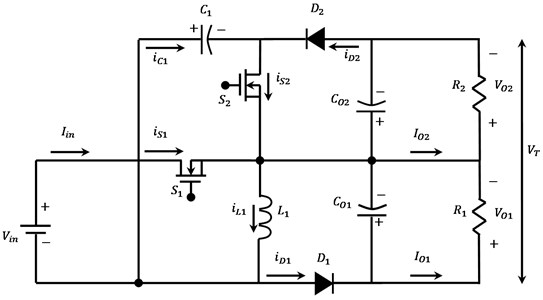
Fig. 3 illustrates the newly introduced single input multi-output topology that can carry out both of the step up and step-down conversions. DOBB converter offers versatility due to its capabilities in improving the dynamic response during the input voltage and load disturbances. Moreover, for applications where in there is a prior information or predictability regarding the load or input voltage disturbance, DOBB possesses the capability to eliminate the impact of these disturbances from the output voltages. Further, the new topology might act as sign priorities to the output voltages in order to attain a better dynamic performance in which the sensitive loads are provided in addition to loads that frequently vary.
Fig. 3Proposed DOBB converter
In the present research, a DOBB converter topology is suggested with the following significant features.
• Any number of passive loads could be included.
• DOBB can work both in Continuous Conduction Mode (CCM) and Discontinuous Conduction Mode (DCM).
• The power supplied by input DC source can be controlled; therefore, the power budgeting between input energy source and load can be combined.
• DOBB uses only a single inductor that can help in reducing the complexity and the expense of the system in addition to simplifying the current sensing.
• The output voltages can be greater compared to the maximum input voltage or lesser in comparison to the minimum input voltage.
• Possibility of a symmetrical or asymmetrical voltage balancing of output capacitor voltage is present in this DOBB converter.
In Fig. 3, the new converter with Single-Input Two-Output is illustrated. This circuit comprises a BB switch (S1), power sharing switch (S2), two power diodes (D1 and D2), a single BB inductor (L1), intermediate capacitor (C1) and output capacitors (C01 and C02) with two different kinds of loads (R1 and R2). As shown in the above figure, (R1) and (R2) refer to the model of load resistances, which can indicate the equivalent power supplying 40 W load. Two power switches,S1 and S2, in the converter structure act as the chief controllable elements, which regulate the power flow and the output voltages of the converter. For every switch, a certain responsibility are given. The BB switch (S1) is active in order to control the inductor (L1) current to the value desired. Actually, S1 controls the capacitor (C01) voltage to the necessary value by regulating the inductor (L1) current. Control of the total output voltage (Vout=V01+V02) to necessary value is the responsibility of the power sharing switch (S2). Gate signals of switches and the current waveforms of inductor, switches, diodes and capacitors are illustrated in Fig. 4. Based on the states of the switches, there are three various operation modes in the whole switching period as shown below.
Fig. 4Key waveforms of the proposed DOBB converter
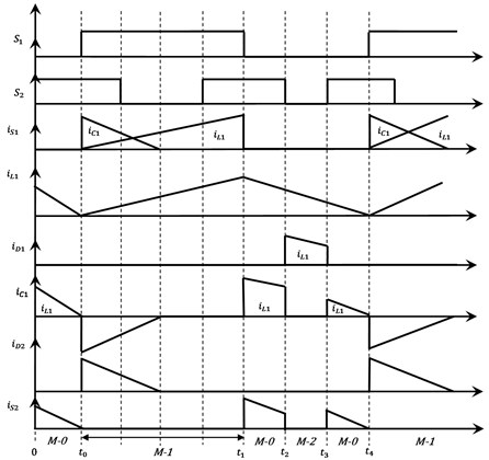
2.1.1. Switching state 1 [0 to t0 (or) t1 to t2]
In switching state 1, the switch (S2) is turned ON. As (S2) is ON, diodes (D1 and D2) are reverse biased, therefore the switch (S1) is turned OFF. The equivalent circuit of the new converter in this state is illustrated in Fig. 5. In this switching state, an inductor (L1) current charges the capacitor (C1) so that the inductor current reduces and capacitor (C1) current faces a rise. Moreover, in this mode, capacitors (C01 and C02) get discharged and supply their stored energy to the load resistances (R1 and R2) correspondingly as illustrated in Fig. 4. In this mode the inductor and capacitor current and voltage are expressed by Eq. (1) below:
Fig. 5Switching state 1 [0 to t0 (or) t1 to t2]
![Switching state 1 [0 to t0 (or) t1 to t2]](https://static-01.extrica.com/articles/19228/19228-img8.jpg)
2.1.2. Switching state 2 [t0tot1]
In switching state 2, switch (S1) is turned ON. As (S1) is ON, diode (D2) gets forward biased so that the switch (S2) is turned ON/OFF. The equivalent circuit of the converter proposed in this state is illustrated in Fig. 6. In this state of switching input DC source (Vin) charges the inductor (L1), and hence the inductor current sees an increase. At the same time, intermediate capacitor (C1) and input dc source (Vin) delivers/discharges its energy to the output capacitor (C02) through diode (D2). In addition, in this mode, capacitors (C01 and C02) get discharged and their stored energy is delivered to the corresponding load resistances (R1 and R2) as illustrated in Fig. 4. In this mode, the current and the voltage of the inductor and capacitors are expressed as in Eq. (2) below:
Fig. 6Switching state 2 [t0 to t1]
![Switching state 2 [t0 to t1]](https://static-01.extrica.com/articles/19228/19228-img9.jpg)
2.1.3. Switching state 3 [t2to t3]
In switching state 3, both the switches (S1 and S2) are turned OFF. Therefore, the diode (D1) is forward biased. The equivalent circuit of the new converter in this state is illustrated in Fig. 7. In this switching state, an inductor (L1) current charges the capacitor (C01), hence the inductor current reduces and capacitor (C01) current rises. In addition, in this mode, capacitors (C01 and C02) get discharged and supply their stored energy to the respective load resistances (R1 and R2) as illustrated in Fig. 4. The current and voltage of the inductor and capacitors are expressed by Eq. (3) below:
From the above Eqs. (1), (2) and (3) it is noted that the capacitor, inductor charges/delivers the voltages at different switching modes of operation.
Fig. 7Switching state 3 [t2 to t3]
![Switching state 3 [t2 to t3]](https://static-01.extrica.com/articles/19228/19228-img10.jpg)
2.2. Control strategy of DOBB converter
The control mechanism is designed in order to achieve a stable voltage and control current storage capability of the topology in order to improve the dynamic response of the converter during the application of the load or input voltage disturbances. In the situation of rise in input voltage or drop in load current that may result in over-voltage in the output, closed loop regulation that senses the actual output voltage of the system and then activates the power switches in order to deviate the inductor current from the load and to eliminate the over-voltage is required. The case of drop in input voltage or rise in load current is also solved by using of closed loop control strategies. The contribution done by the present research depends up on the SIMO DOBB converter by selecting a classical Proportional Integral (PI) controller for a closed loop control strategy. The PI controller attempts to precise the error among the measured process variables and the desired set point through calculation and then provides an accurate output, consequently it can control the conversion process.
The PI controller computation involves two unique modes: proportional mode and integral mode. In the proportional mode, the reaction to the current error is decided, but in the integral mode, the reaction based recent error is decided. The weighted sum of the two modes provides the output to be the corrective action to the control element. PI controller is widely applied in several industries due to its simple design and unsophisticated structure. PI controller algorithm can be run by Eq. (4):
where means err(t)= set voltage-actual voltage.
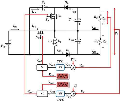
A voltage follower approach is adjustable for controlling the DOBB converter when it operates with DCM. A dual voltage sensors, i.e. total output voltage and capacitor (C01) voltage measurement sensors, is necessary for regulating output voltage of the DOBB converter. Fig. 8 presents a closed loop control of the DOBB converter. This control strategy comprises a voltage error generator, Output Voltage Controller (OVC), Capacitor Voltage Controller (CVC) and a PWM generator.
The error generator of OVC compares of the preferred output voltage (V*out) of DOBB converter with the original output voltage (Vout) for generating an error voltage (Vce1), provided in Eq. (5). In the same way, the error generator of CVC does the comparison of this DOBB converter capacitor (C01) voltage (V*01) with the original output voltage (V01) so as to produce an error voltage(Vce2), provided by Eq. (6):
where ‘k’ indicates the kth sampling instance. This error voltage (Ve1) and (Ve2) is delivered to an OVC and CVC for generating a regulated total output voltage (Vce1), and regulated capacitor output voltage (Vce2), given in Eq. (7) and (8) respectively:
where Kp and Ki refer to the respective proportional and integral gains of the PI controller. At last, the generation of the PWM signals are done by making a comparison between the output of OVC and CVC with the high-frequency saw-tooth signal (Vcar), that generates the gate signals (Vgs1 and Vgs2) to DOBB converter switches (S1 and S2).
Fig. 8Closed loop control of DOBB converter
2.2.1. Estimation of power losses in DOBB converter
The efficiency of system is indirectly proportional to the total power losses. The total power losses, in the DOBB converter, are the conduction, switching, diode and inductor losses. Occurrence of the conduction losses is due to the declining voltage across the device as well as the current flow through the device striking in chorus. Switching losses are sustained by the concurrent occurrence of voltage and current on the device while switching. The key waveforms of DOBB converter are shown in Fig. 9. Iin, iL1, iD1, iD2, and iC1 are the current through the input supply, inductor L1, diodes D1 and D2, and capacitor C1 respectively. Evaluation of these losses can be done using simplified device models.
2.2.2. Calculation of switching losses of BB switch (S1) in DOBB converter
2.2.2.1. Conduction loss of switch (S1)
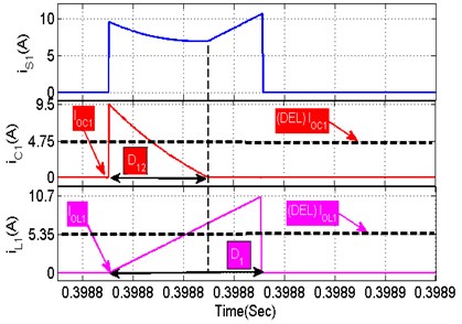
To analyze the conduction loss of switch (S1), the device is simplified to be a stable voltage drop that is in series with a linear resistor (RDS on = 0.07). RDS on is based on the applied Gate Source Voltage (VGS) and the junction temperature. The conduction loss of switch (S1) is expressed in Eq. (9):
where (IS1) indicates the current flowing through the switch (S1), (IS1) is further divided by the respective inductor current (IS1L1) and capacitor current (IS1C1) flowing through the switch (S1). The current conduction of switch (S1) is expressed in Eq. (10):
where () indicates the “ON” time of switch (), () represents the capacitor () discharged time at (), () and () stand for the inductor and capacitor current at the beginning. Then () and () stand for the respective average ripple current of inductor and capacitor as expressed in Eq. (11):
where (), () represents the maximum and minimum amplitude of inductor () current. In the same way (), () represents the maximum and minimum amplitude of capacitor () current as illustrated in Fig. 9. It is evidently noticed from Fig. 10, that 0.3, 0.2, 0, 0, 5.35 and 4.75. These values are substituted in Eq. (10) and Eq. (9), and the total current conduction and conduction loss of BB switch () as resolved in Eq. (12):
Fig. 9Open loop key waveforms of DOBB converter
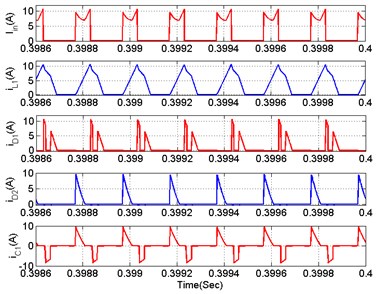
Fig. 10Representation of key waveforms during switch (S1)
2.2.2.2. Turn-on and turn-off losses of switch ()
Turn-on losses are defined to be an exposure of the component to a considerable amount of voltage and the current experienced simultaneously when the device turned on. In the same way, turn-off losses can also be defined to be an exposure of the component to a considerable amount of voltage and the current simultaneously experienced when the device is turned-off. Switching losses are produced as a consequence of a Metal Oxide Semiconductor Field Effect Transistor (MOSFET) simultaneously getting exposed to a high voltage and current while a transition happens between the open and the closed states. Hence it is enough to know about the duration and the kind of a transition, for instance resistive or inductive. The electrical characteristics of switch IRFZ24N ( 34 , 27 , 18 V) are utilized for simulation study and calculation of theoretical efficiency. The Turn-on and Turn-off of Losses () is computed by Eq. (13):
where is Rise time, is Fall time, refers to Current conduction of switch () (refer Eq. (12)), stands for drain voltage of switch () and, is operating switching frequency (5 kHz).
The total power losses of switch () is expressed in Eq. (14):
2.2.3. Calculation of losses in power sharing switching () in DOBB converter
2.2.3.1. Conduction loss of switch ()
To analyze the conduction loss of , the device is simplified to be a stable voltage drop that is in in series with a linear resistor (RDS on = 0.07). RDS on is based on the applied VGS and the junction temperature. The conduction loss of switch () is expressed in Eq. (15):
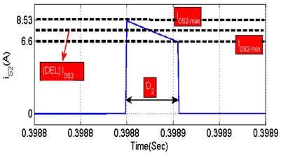
where () indicates the current flowing through the switch (), () stands for the “ON” time of switch (), () represents the switch () current at time of starting, and () stands for the average ripple current of switch (). The switch current at the beginning instant () is derived from Eq. (16):
The average ripple current () is observed from Eq. (17):
where (), () represents maximum and minimum amplitude of switch () current as illustrated in Fig. 10. It is seen from Fig. 11, that 0.22, 7.565 and 0.965, which are substituted in Eq. (15), the total current conduction and conduction loss of power sharing switch () as resolved in Eq. (18):
Fig. 11Representation of key waveform during switch (S2) conduction
2.2.3.2. Turn-on and turn-off losses of switch ()
The electrical characteristics of switch IRFZ24N ( 34 ns, 27 ns, 34 V) are utilized for the purposes of simulation studies and calculation of theoretical efficiency. The switch () Turn-on and Turn-off losses () is computed by Eq. (19):
where refers to current conduction of switch () (refer Eq. (18)), is: drain voltage of switch () and is Operating switching frequency (10 kHz)
The total power losses of switch () is obtained from Eq. (20):
2.3. Loss of diode () in DOBB converter
For the diode (), the loss due to forward voltage ( 0.8) is expressed by Eq. (21):
where () indicates the current flow through the diode (), () stands for the “ON” time of diode (), () refers to the diode () current at the time of starting and () stands for the average ripple current of diode (). The diode current at the beginning instant () equals to zero, therefore the average ripple current () is obtained from Eq. (22):
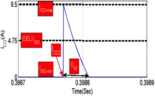
where (), () indicates the maximum and minimum amplitude of diode ( current as illustrated in Fig. 11. It can be seen clearly from Fig. 12, that 0.15, 0 and 3.25. These values are substituted in Eq. (21), the total current conduction and the power loss of diode ( as resolved in Eq. (23):
2.4. Loss of diode () in DOBB converter
For the diode (), the loss due to forward voltage ( 0.8) is provided by Eq. (24):
where () indicates the current flow through the diode (), () stands for the “ON” time of diode (), () refers to the diode () current at the time of starting, and () stands for the average ripple current of diode (). The diode current at the instant () of starting equals to zero, hence the average ripple current () is derived from Eq. (25):
where (), () represent the maximum and minimum amplitude of diode ( current as illustrated in Fig. 13. It is observed from Fig. 12 that 0.19, 0 and 4.75. These values are substituted in Eq. (24), the total current conduction and the power loss of diode ( as is done in Eq. (26):
2.5. Loss of inductor () in DOBB converter
Losses in an inductor are contributed by two factors. One factor is the wire loss and the second one is the core loss. The loss because of the wire is provided by Eq. (27):
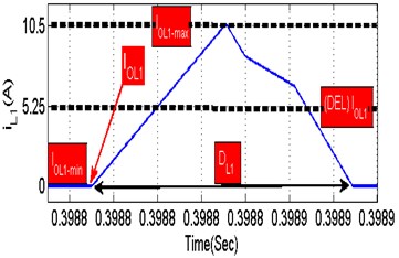
where () stands for the current flow through the inductor (), () indicates the “ON” time of inductor (), () refers to inductor () current at time of starting, ( 0.9) stands for the equivalent dc resistance of 0.1 mH Ferrite core inductor and () refers to the average ripple current of inductor ().
Fig. 12Representation of key waveform during the conduction of diode (D2)
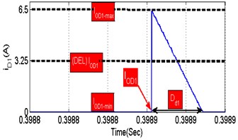
Fig. 13Representation of key waveform during diode (D2) conduction
The inductor current at the instant of starting () equals to zero, therefore the average ripple current () is observed from Eq. (28):
where (), () represent the maximum and minimum amplitude of inductor ( current as illustrated in Fig. 14. shows clearly that 0.67, 0 and 5.25. These values are substituted in Eq. (27), the total current conduction and power loss of inductor ( are resolved in Eq. (29):
2.6. Total power losses in DOBB converter
The total power losses in DOBB converter is the summation of all the factors mentioned above. The total power losses () and system efficiency can be calculated making use of Eq. (30):
where, Output power of DOBB converter (40 W) and refers to total power losses
Fig. 14Representation of key waveform during the conduction of inductor (L1)
3. Results and discussion
To find out the performance of the proposed converter under the present control strategy, MATLAB simulations in different conditions with symmetrical and asymmetrical output voltage variation have been performed.
The simulation parameters such as input voltage (), input current (), first output voltage, current and power of DOBB converter (, and ) respectively, second output voltage, current and power of DOBB converter (, and ) respectively and total output voltage () and total power () are used to evaluate the performance of the proposed system as shown in Table 1.
Table 1Simulation parameters for DOBB converter
Components and symbols | Parameters |
Input inductor () | 389.4 μH |
Intermediate capacitor () | 50 μF |
Output capacitors ( and ) | 1000 μF, 100 V |
Operating switching frequency () of switches | 5 kHz, 10 kHz |
Load resistances ( and ) | 28.8 Ω |
3.1. Symmetrical output voltage control of DOBB converter
To verify the symmetrical performance of DOBB converter, input dc voltage source is considered as ( 18 V) as shown in Fig. 15(a). The output voltages of the DOBB converter are desired to be regulated on (24 V and 24 V). Consequently, the total output voltage and total power are desired to be regulated on ( 48 V) and ( 40 W). Moreover, load resistances ( 28.8 Ω) are considered for symmetrical condition.
Fig. 15Performance of DOBB converter under symmetrical voltage condition

a)

b)

c)

d)

e)

f)

g)

h)

e)
In Figs. 15(c) and (d), output voltages ( and ) are shown. As seen from this figure, the output voltages are tracked with the references values ( and 24 V) with minimum steady state error. It is obvious that the output voltages are regulated very well. Similarly, the currents ( and ) drawn from load resistances and are shown in Figs. 15(e) and (f), both the loads consume 20 W power from input supply individually. Therefore, the power drawn from load resistances and are shown in Figs. 15(g) and (h). In Fig. 15(i), the total output voltage () and total output power () are shown. As seen from this figure, voltage and power are tracked with the reference values ( 48 V and 40 W). It is obvious that the output voltage and power are regulated smoothly. Thus, the 40 W loads draw current from input dc source as is revealed in Fig. 15(b).
Fig. 16Output voltage ripple evaluation of proposed DOBB converter
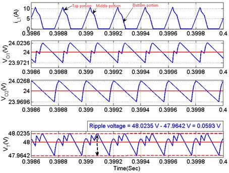
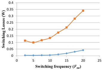
Moreover, two different switching frequencies of switches ( 5 kHz and 10 kHz) are desired to be separate the inductor discharging current as three portions. The top and bottom portion of inductor current , energies the output capacitor (). The middle portions of inductor current , energies the output capacitor (). Thus, it will reduce the output ripple considerably as shown in Fig. 16. Moreover, switching losses and conduction losses of switch and are analysed with respective switching frequency and duty cycle as shown in Fig. 17. The switching frequency of the solid-state switches is kept on the order of 5 kHz, 10 kHz for proper operation. Such high switching frequency causes high switching losses in the switch .
Fig. 17Analysis of losses in switches S1 and S2 with respective switching frequency and duty cycle
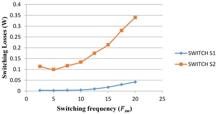
a) Switching losses vs. Switching frequency
b) Conduction losses vs. Duty cycle
3.2. Simulated comparison of two conventional converter with the proposed DOBB
To identify the limitations of conventional converters Nami et al. [7] and Boora et al. [8], the output voltages of the conventional converters are desired to be regulated on ( 24 V, 24 V i.e. 48 V) from 0 to 0.4 Sec. After 0.4 sec, the output voltages are desired to be regulated on ( 18 V, 30 Vi.e. 48 V) respectively as shown in Figs. 18 and 19. For this analysis input dc voltage source is considered to be 18 V and load resistances are considered to be 28.8 OHM.
Fig. 18Figure performance of Nami et al. (2010) converter when V01<V02
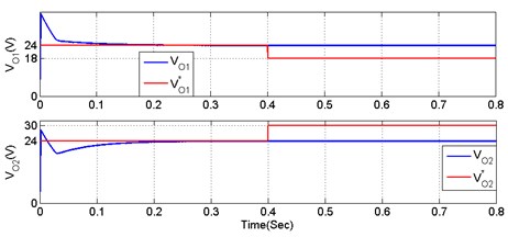
Fig. 19Performance of [8] converter
![Performance of [8] converter](https://static-01.extrica.com/articles/19228/19228-img31.jpg)
Observing from Figs. 18 and 19 conventional converters [7, 8] output voltages ( 24 V, 24 V i.e. 48 V) are regulated very well at symmetrical condition. But in asymmetrical condition, which is , not able to follow the output voltage as proved. Because the output capacitor () has the individual charging ability but another capacitor () does not have the individual charging ability. Alternatively, the proposed DOBB converter has the individual charging ability of both capacitors (, ). Therefore, DOBB converter follows the reference voltages at both symmetrical and asymmetrical conditions as shown in Fig. 20.
Fig. 20Performance of DOBB converter
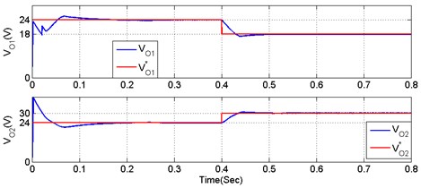
Table 2Voltage control ability of conventional and proposed converters
Converter presented by [7] | ||||
Switching states | States of output capacitors | |||
– | ||||
1 | 0 | – | Discharge | Discharge |
0 | 0 | – | Charge | Charge |
0 | 1 | – | Charge | Discharge |
Converter presented by [8] | ||||
Switching states | States of output capacitors | |||
0 | 0 | 0 | Charge | Charge |
0 | 0 | 1 | Charge | Discharge |
0 | 1 | 0 | Discharge | Discharge |
1 | 0 | 1 | Charge | Discharge |
1 | 0 | 0 | Charge | Charge |
1 | 1 | 0 | Discharge | Discharge |
Proposed DOBB converter | ||||
Switching states | States of output capacitors | |||
– | ||||
0 | 1 | – | Charge | Discharge |
1 | 0 | – | Discharge | Charge |
0 | 0 | – | Charge | Discharge |
The voltage control ability of conventional and proposed converters is estimated using Table 2. It is obvious from the table that in [7] the output voltage () is greater than () the reason is that the output capacitor () has the individual charging ability at switching states (0, 1), but the output capacitor () does not have the individual charging ability at all the three switching states, therefore second output voltage () always depends on first output voltage (). Similarly, in the study by [8] the output capacitor () has the individual charging ability at switching states (0, 0, 1) and (1, 0, 1). But the output capacitor () does not have the individual charging ability at all the six switching states, therefore second output voltage () always depends up on the first output voltage (). Moreover, in [8] not able to control the output voltage () is greater than () but in DOBB converter the output capacitors () and () have the individual charging ability at switching states (0, 1) and (1, 0) respectively. It is one of the main advantages of the proposed DOBB converter.
The proposed DOBB converter topologies are compared with respect to their component count, type of conversion, possibility of output voltage control, switching states and driver circuit complexity. Table 3 presents a comparison between topologies of interest. It should be noted that the converter presented by [7] has the lowest number of semiconductor devices in the current conduction path. However, it has three main disadvantages: a step-up conversion is only possible, the second output voltage () always equal/lesser than the first output voltage (), and separate grounding of switches leads to an individual power supply for driver circuit. Similarly, the converter presented by [8] has three main disadvantages: a higher component count, the second output voltage () is always equal/lesser than the first output voltage () and separate grounding of switches. Finally, these disadvantages can be minimized by implementing DOBB converter which has many advantages: step-up and step-down conversions are possible, lower component count and both the output capacitor voltages ( or ) is controllable. Further common grounding switches present in DOBB converter reduces power supply, noise emission problems and improves the efficiency of it.
Table 3Performance comparison of the conventional and proposed DOBB converters with various objects
Various dual output converters | |||
Objects | Converter presented by [7] | Converter presented by [8] | Proposed DOBB converter |
Total number of switches | 2 | 3 | 2 |
Total number of diodes | 2 | 3 | 2 |
Total number of capacitors | 2 | 2 | 3 |
Total number of inductors | 1 | 1 | 1 |
Total number of components | 7 | 9 | 8 |
Type of conversion | (Step-up) | (Both step-up and step-down) | (Both step-up and step-down) |
Switching states complexity | Simple | Complex | Simple |
Driver circuit complexity | Medium | Complex | Simple |
Table 4Time domain analysis of output voltage under step change in input and load conditions
Step change in | (v) | Applied load in % | (v) | Over shoot (v) | Rise time (ms) | Settling time (ms) | Steady state error (mv) | Delay time (ms) |
Input | 18 | 100 | 0-48 | 15 | 2.44 | 124 | 340 | 1.5 |
36 | 100 | 48 | 7 | – | 93 | 460 | – | |
Load | 18 | 100 | 0-48 | 14 | 2.4 | 124 | 340 | 1.5 |
18 | 50 | 48 | 1.1 | 1.7 | 48 | 250 | – |
3.3. Algorithm of repetitive control and feedforward compensation control
The repetitive compensator is the compensator which adds the input signal to the output one which delays the input one by only one cycle . In this research, in order to realize the repetitive compensator by DSP, we have to design it by the discrete system. Fig. 5 shows the fundamental operation of the repetitive compensator and the time leading element in the discrete system. As shown in Fig. 5, the repetitive compensator consists of memories, and in the case the control period is , and the relation of is derived. As this control system, in the case the period of the input signal (ripple torque) synchronizes with the rotation speed of the brushless DC motor, the number of N also change with change of , in the system fixed the control period inconveniently. Then, is allowed to change and the repetitive compensator with memories in one period is realized by synchronizing the control period with the rotation angle of the rotor . The input signal to the repetitive compensator (= the output signal from the proportional compensator) is averaged within the period of and added to the data in the corresponding memory.
3.4. Experimental results of the proposed DOBB
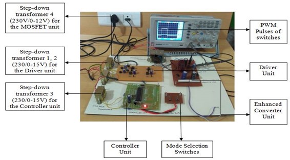
For verifying the efficiency of the system proposed, a low power range laboratory prototype is constructed as illustrated in Fig. 21. For the experimental arrangement, two diverse input power sources are used. A power supply with the electric specification of 18 V, 2.386 A and 42.96 W, are considered to be the input power source. The prototype parameters of proposed system are given in Table 5.
Table 5Experimental specification of the proposed DOBB
S. No | Objects | Values |
1 | DC power source | 18 V, 0.83 A and 42.96 W |
2 | Converter output voltage | 48 V |
3 | Converter output current | 0.83 A |
4 | Converter output power | 40 W |
Fig. 21Prototype model of proposed DOBB converter system
3.5. Performance of capacitor
The input voltage (230 V) is step down to (18 V) using the transformer and converted to DC with the help of bridge rectifier and the input is fed to controller with the help of voltage regulator. The output voltage from controller is given to enhanced converter unit and the output voltage across the individual capacitor is displayed using the DSO. Fig. 22 shows the output waveform of the capacitor.
3.6. Performance of capacitor
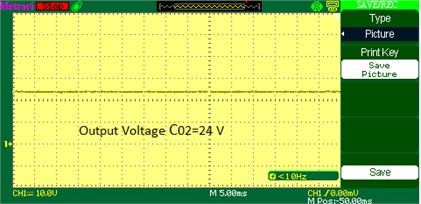
The input voltage (230 V) is step down to (18 V) using the transformer and converted to DC with the help of bridge rectifier and the input is fed to controller with the help of voltage regulator. The output voltage from controller is given to enhanced converter unit and the output voltage across the individual capacitor is displayed using the DSO. Fig. 23 shows the output waveform of the capacitor.
3.7. Performance of switch in boost mode
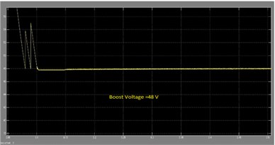
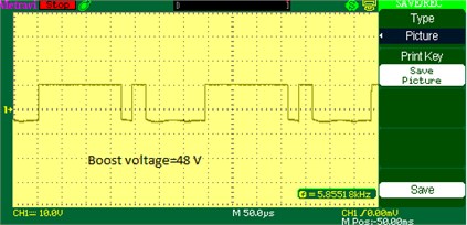
Fig. 24 shows the output waveform of PWM Pulses across the switches in the Boost mode. These PWM pulses are generated by driver circuit by means of the mode selection switches connected along with the microcontroller.
Fig. 22C01 output voltage waveform of DOBB converter: a) simulation b) experimental waveform

a)

b)
Fig. 23C02 output voltage waveform of DOBB converter: a) simulation, b) experimental waveform

a)
b)
Fig. 24Boost voltage waveform of DOBB converter: a) simulation, b) experimental waveform PWM pulses across the switch S1 in boost mode
a)
b)
3.8. Performance of switch in buck mode
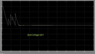
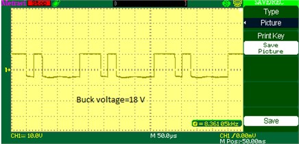
Fig. 25 presents output Pulses across the switches in the Buck mode. These PWM pulses are generated by driver circuit by means of the mode selection switches connected along with the microcontroller.
Fig. 25Buck voltage waveform of DOBB converter: a) simulation, b) experimental waveform PWM pulses across the switch S1 in buck mode
a)
b)
3.9. Performance of switch in boost mode
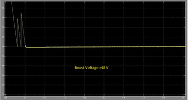
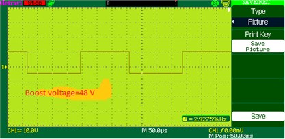
Fig. 26 shows the output Pulses across the switches in the Boost mode. These PWM pulses are generated by driver circuit by means of the mode selection switches connected along with the microcontroller.
Fig. 26Boost voltage waveform of DOBB converter: a) simulation, b) experimental waveform PWM pulses across the switch S2 in boost mode
a)
b)
3.10. Performance of the switch in buck mode
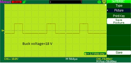
Fig. 27 presents the output Pulses across the switches in the Buck mode. These PWM pulses are generated by driver circuit by means of the mode selection switches connected along with the microcontroller.
Fig. 27Buck voltage waveform of DOBB converter: a) simulation, b) experimental waveform PWM pulses across the switch S2 in buck mode

a)
b)
4. Conclusions
In this paper, a new structure of DOBB and frequency components of vibrations has been proposed. The proposed topology extends the design flexibility and the possibility to optimise the power converter for achieving the main objectives. Compared with conventional inverter systems, the proposed system is employed with reduced voltage stress, reduced switch count and DC source count. The proposed DOBB configuration required at least two DC sources for Converter Exhaustive operations are carried out, switching losses are calculated, simulation results are carried out for symmetrical and asymmetrical output voltage. The proposed DOBB Converter is compared with the conventional one and finally, it is proved to be more efficient than the other conventional converters. In addition, the proposed methods were examined in the case of low speed drive of the brushless DC motor. However, for the higher order frequency components of the vibration and those near the sharp resonance frequency of the mechanical system, the effectiveness of the proposed vibration suppression method was small. Several analyses in terms of cost, semiconductor loss and harmonics have been made and it is inferred that the proposed structure can be an appropriate aspirant for power converters used in industrial and drive applications.
References
-
Pan C. T., Cheng M. C., Lai C. M. A novel integrated dc/ac converter with high voltage gain capability for distributed energy resource systems. IEEE Transactions on Power Electronics, Vol. 27, Issue 5, 2012, p. 2385-2395.
-
Ellis M. W., Von Spakovsky M. R., Nelson D. J. Fuel cell systems: efficient, flexible energy conversion for the 21st century. Proceedings of the IEEE, Vol. 89, Issue 12, 2001, p. 1808-1818.
-
Gao F., Blunier B., Sim˜oes M. G., Miraoui A. PEM fuel cell stack modeling for real-time emulation in hardware-in-the-loop application. IEEE Transactions on Energy Conversion, Vol. 26, Issue 1, 2011, p. 184-194.
-
Ma D., Ki W.-H., Tsui C.-Y. A pseudo-CCM/DCM SIMO switching converter with freewheel switching. IEEE Journal of Solid-State Circuits, Vol. 38, Issue 6, 2003, p. 1007-1014.
-
Trevisan D., Mattavelli P., Tenti P. Digital control of single-inductor multiple-output step-down dc-dc converters in CCM. IEEE Transactions on Industrial Electronics, Vol. 55, Issue 9, 2008, p. 3476-3483.
-
Chakraborty S., Jain A. K., Mohan N. A novel converter topology for multiple individually regulated outputs. IEEE Transactions on Power Electronics, Vol. 21, Issue 2, 2006, p. 361-369.
-
Nami A., Zare F., Ghosh A., Blaabjerg F. Multiple-output DC-DC converters based on diode-clamped converters configuration: topology and control strategy. IET Power Electronics, Vol. 3, Issue 2, 2010, p. 197-208.
-
Boora A., Zare F., Ghosh A. Multi-output buck-boost converter with enhanced dynamic response to load and input voltage changes. IET Power Electronics, Vol. 4, Issue 2, 2011, p. 194-208.
-
Boora A., Nami A., Zare F., Ghosh A., Blaabjerg F. Voltages haring converter to supply single-phase asymmetrical four-level diode-clamped inverter with high power factor loads. IEEE Transactions on Power Electronics, Vol. 25, Issue 10, 2010, p. 2507-2520.
-
Patra P., Patra A., Misra N. A single-inductor multiple-output switcher with simultaneous buck, boost and inverted outputs. IEEE Transactions on Power Electronics, Vol. 27, Issue 4, 2012, p. 1936-1951.
-
Solero L., Caricchi F., Crescimbini F., Honorati O., Mezzetti F. Performance of a 10 kW power electronic interface for combined wind/PVisolated generating systems. Conference on Power Electronics Specialists, 1996, p. 1027-1032.
-
Kirubakaran A., Jain S., Nema R. K. DSP-controlled power electronic interface for fuel-cell-based distributed generation. IEEE Transactions on Power Electronics, Vol. 26, Issue 12, 2011, p. 3853-3864.
-
Chen Y., Kang Y., Nie S., Pei X. The multiple-output DC-DCconverter with shared ZCS lagging leg. IEEE Transactions on Power Electronics, Vol. 26, Issue 8, 2011, p. 2278-2294.
-
Dobbs B. G., Chapman P. L. A multiple-input dc-dc converter topology. IEEE Transactions on Power Electronics, Vol. 1, Issue 1, 2003, p. 6-9.

